Active production — sourcing and compliance
The TLV70736PDQNR: No stock-holding claim — each RFQ is handled individually.
Fixed 3.6 V output at 200 mA continuous — this is a clean rail for powering low-voltage RF front-ends, sensor analog supplies, or the core of a BLE SoC that runs on a 3.3 V nominal bus but needs margin for dropout. The 0.25 V max dropout at 150 mA means the input must stay above 3.85 V to hold regulation at that load; at 200 mA the dropout will be higher, so budget 4.0 V minimum input for full output. Quiescent current is 50 µA typical — low enough that a battery-powered sensor node logging once per minute sees negligible overhead from the regulator itself. The enable pin lets the host MCU gate the rail entirely, dropping Iq to near zero in sleep mode.
PSRR across the band — noise rejection that matters for RF
PSRR is specified at 70 dB at 100 Hz, rolling off to 50 dB at 1 MHz. That 50 dB at 1 MHz is the figure that matters for a Wi-Fi or BLE radio drawing pulsed current at the packet rate — the regulator attenuates switching noise from a buck converter upstream by a factor of ~300 at that frequency, keeping the spur floor low enough to avoid desensitising the receiver. Below 100 Hz, mains ripple is rejected by a factor of 3000.
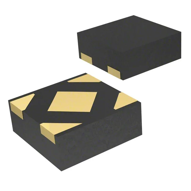
Package and board-fit — 4-X2SON (1x1 mm)
The 0.5 mm pitch is fine for a standard 2-layer board with 0.2 mm trace/space, but the exposed pad needs a via array to the ground plane for heat spreading. The protection set includes over-current, over-temperature, short-circuit, and reverse polarity; the reverse polarity clamp is unusual at this current level and saves an external Schottky diode on the input if the supply can be reversed.