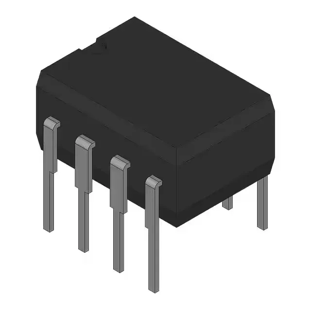
Texas Instruments TLV2422MJGB — Logic ICs

TLV2422MJGB Dual Op-Amp, 5.3 MHz, AEC-Q100, CDIP-8

MPNTLV2422MJGB
End of Life

Texas Instruments TLV2422MJGB, Automotive AEC-Q100 LinCMOS™ dual general-purpose op-amp, 5.3 MHz GBW, 0.02 V/µs slew rate, rail-to-rail output, 100 µA supply per channel, -55 to 125°C, 8-CDIP through-hole package.

$11.87Ref. price · indicative, final on quote
Packaging8-CDIP (0.300", 7.62mm)
StockContact for availability
MOQ1 pcs
  • 100% new & originalTraceable channels only — no refurbs, no pulls, no remarked parts.
  • Date & lot codes on quoteStated per line before you commit; label photos on request.
  • MSL-compliant ESD packingMoisture-sealed bags with indicator cards; reels photo-verified.
  • PayPal buyer protectionPay by T/T, PayPal or Payoneer — card payments covered end to end.

Specifications

TLV2422MJGB Technical Specifications
ParameterValue
SeriesAutomotive, AEC-Q100, LinCMOS™
Output typeRail-to-Rail
Mounting typeThrough Hole
Amplifier typeGeneral Purpose
Voltage - input offset300 µV
Voltage - supply span2.7 V
Current - supply100µA (x2 Channels)
Current - input bias1 pA
Current - output (Channel)50 mA
Operating temperature-55°C ~ 125°C
Gain bandwidth product5.3 MHz
PackageBulk
Slew rate0.02V/µs
Case8-CDIP (0.300\", 7.62mm)
Number of circuits2

Product details

The rail-to-rail output stage maximizes dynamic range at low supply voltages, and the 1 pA input bias current suits high-impedance sensor interfaces.

Hermetic CDIP-8 — why the package matters

This part comes in an 8-pin ceramic dual-in-line package (8-CDIP, 0.300" body width), through-hole mount. The hermetic ceramic construction resists moisture and outgassing, so it is a natural choice for sealed assemblies, avionics, downhole tools, or any environment where a plastic SOIC would risk reliability. No moisture-sensitivity level (MSL) concern — store the tubes on the shelf, no bake required before reflow if the assembly process uses a solder pot or hand-solders the leads.

Operates from a single supply as low as 2.7 V up to 10 V maximum. The 300 µV input offset voltage (maximum) is typical for a CMOS-input amplifier in this class — no auto-zero, but adequate for general-purpose signal conditioning where you are not amplifying microvolt-level signals.

Lifecycle and sourcing posture

It is RoHS non-compliant (the hermetic package uses lead-bearing solder dip on the leads), so factor that into any EU RoHS exemption paperwork.

Frequently asked questions

What is the TLV2422MJGB equivalent or replacement?

No pin-compatible drop-in replacement is listed. The TLV9362IDDFR is a newer surface-mount dual op-amp with higher bandwidth (10.6 MHz) and faster slew rate (25 V/µs), but it comes in a plastic SOIC package and is not a direct footprint or temperature-range match for the hermetic CDIP-8 TLV2422MJGB.