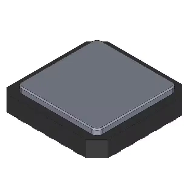
JFET op-amp in a hermetic ceramic LCC — what this package tells you
The JFET input stage delivers 20 pA typical input bias current, which preserves signal accuracy when the source impedance is high, such as photodiode preamps or piezoelectric sensor buffers.
45 V/µs slew rate — large-signal bandwidth and settling
The 45 V/µs slew rate, combined with a 10 MHz gain-bandwidth product, means this op-amp can swing a 10 V peak-to-peak output at frequencies up to roughly 700 kHz without slew-rate limiting. That makes it suitable for fast-settling data-acquisition front ends, waveform generation, and audio line drivers where preserving transient integrity matters. The 48 mA output current per channel gives enough drive to handle a 600 Ω load or a modest capacitive load without external buffer stages.
Supply range and input offset — design margins
The supply span runs from 4.5 V to 38 V, so the part works on a single 5 V rail or split ±15 V supplies common in precision analog systems. Quiescent supply current is 1.6 mA per amplifier, which keeps the thermal budget manageable in the ceramic package.