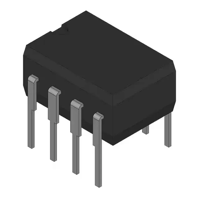
Hermetic JFET op-amp for extreme environments
It combines a 2 MHz gain-bandwidth product with a 3.4 V/µs slew rate and draws 625 µA per channel. The J-FET input stage delivers 4 pA input bias current and 900 µV input offset voltage. Output stage can source or sink 80 mA per channel. Supply range spans 7 V to 36 V single or dual supply.
Why the 8-CDIP package matters
The 8-CDIP (0.300", 7.62 mm) ceramic dual-in-line package is the through-hole, hermetic option for designs that must survive humidity, thermal cycling, and outgassing constraints. This is not a plastic SOIC or PDIP — the ceramic body and glass-metal seal prevent moisture ingress, making it the standard for MIL-STD-883 screened assemblies and high-reliability programs. Mounting is through-hole only; the leads are tin/lead or gold-plated Kovar depending on the date code lot. Expect a 0.100" pitch footprint compatible with standard DIP sockets or soldered directly into plated through-holes.
Slew rate and bandwidth in the signal chain
At 3.4 V/µs the TLE2062MJG can swing 10 V peak-to-peak in about 3 µs — sufficient for audio, servo loops, and transducer conditioning up to several hundred kHz. The 2 MHz gain-bandwidth product means a closed-loop gain of 10 gives a 200 kHz bandwidth. The 80 mA output current per channel can drive coaxial cables, relay coils, or multiple ADC inputs without an external buffer. The 4 pA input bias current and J-FET topology keep the input impedance above 10¹² Ω, critical for photodiode, pH probe, and piezoelectric sensor front ends where bias current error must stay below a few picoamps.
Active lifecycle — still in production
Independent distribution holds inventory built over multiple date code windows. For new designs targeting military or extended-temperature environments, this is one of the few dual JFET op-amps still available in a hermetic through-hole package.