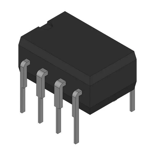
The TLE2061BIP: Its JFET input stage delivers 4 pA typical input bias current, making it suitable for high-impedance sensor interfaces, photodiode amplifiers, and precision integrators where bipolar input current would load the source. The 2 MHz gain-bandwidth product and 3.4 V/µs slew rate cover audio-band filtering, low-speed data acquisition, and control-loop compensation, but it is not a high-speed part for video or RF. Supply current is 290 µA, which keeps the power budget modest in battery-operated or multi-channel systems. The output can source or sink 80 mA, enough to drive headphones, small relays, or a second-stage load directly.
The TLE2061BIP operates from a total supply span of 7 V to 36 V, which translates to single-supply rails from 7 V to 36 V or split supplies from ±3.5 V to ±18 V. The 7 V minimum means it will not run on a single 5 V logic rail; plan for at least a 9 V battery or a ±5 V supply. The through-hole PDIP package is breadboard-friendly and easy to hand-solder, but occupies more board area than a surface-mount SOIC; it is a natural fit for prototyping, repair, and low-volume production where SMD reflow is not available.
This is a stable line item for existing designs. For legacy equipment maintenance, MRO, or designs that are exempt from RoHS, this is not a blocker. The non-compliant status typically means the lead-frame finish contains lead (e.g., SnPb plating), which is still acceptable in military, aerospace, and certain industrial applications under exemption.
Sourcing and availability – how to get TLE2061BIP
Because the part is Active and not subject to allocation or LTB windows, lead times are generally stable. For a firm delivery commitment and quantity pricing, submit an RFQ through the storefront.