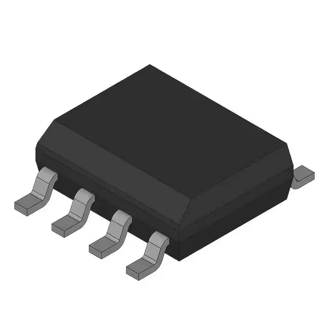
Texas Instruments TLC25L2ACDR — Logic ICs

TI TLC25L2ACDR LinCMOS Op-Amp, 110 kHz, 2.9 V/µs, 8-SOIC

MPNTLC25L2ACDR
End of Life

Texas Instruments LinCMOS™ series, TLC25L2ACDR, dual CMOS op-amp, 110 kHz gain bandwidth, 2.9 V/µs slew rate, 29 µA supply, 1.4 V to 16 V supply range, open-drain output, 8-SOIC package, 0°C to 70°C operating temperature.

$0.84Ref. price · indicative, final on quote
Packaging8-SOIC (0.154", 3.90mm Width)
StockContact for availability
MOQ1 pcs
  • 100% new & originalTraceable channels only — no refurbs, no pulls, no remarked parts.
  • Date & lot codes on quoteStated per line before you commit; label photos on request.
  • MSL-compliant ESD packingMoisture-sealed bags with indicator cards; reels photo-verified.
  • PayPal buyer protectionPay by T/T, PayPal or Payoneer — card payments covered end to end.

Specifications

TLC25L2ACDR Technical Specifications
ParameterValue
SeriesLinCMOS™
Output typeOpen Drain
Mounting typeSurface Mount
Amplifier typeCMOS
Voltage - input offset900 µV
Voltage - supply span1.4 V
Current - supply29µA (x2 Channels)
Current - input bias50 pA
Operating temperature0°C ~ 70°C (TA)
Gain bandwidth product110 kHz
PackageBulk
Slew rate2.9V/µs
Case8-SOIC (0.154\", 3.90mm Width)
Number of circuits2

Product details

Micropower dual op-amp for commercial sensing

The 110 kHz gain-bandwidth product and 2.9 V/µs slew rate handle slow-moving signals like temperature, pressure, or strain-gauge outputs, but it is not intended for high-speed ADC drivers or video paths.

Supply range and output stage

The supply span runs from 1.4 V minimum to 16 V maximum, so a single Li-ion cell or a 12 V industrial rail both work without an intermediate regulator. The open-drain output stage means the part can pull a load to ground but cannot source current — external pull-up resistors are required. This topology suits wired-OR buses, comparator-style interfaces, or level shifting where the output high level is set by an external voltage, not the op-amp's own rail.

Input offset and bias current

Input offset voltage is specified at 900 µV maximum, and input bias current at 50 pA typical. The low bias current is a benefit when the source impedance is high — photodiode or pH probe amplifiers, for instance — because the voltage error from bias current stays small. The offset is moderate; for sub-millivolt precision you would look at a zero-drift amplifier, but for general-purpose signal conditioning it is adequate.

Lifecycle and compliance

It is ROHS3 compliant.

Frequently asked questions

Is TLC25L2ACDR obsolete?

It remains a valid choice for production BOMs, though the commercial temperature grade limits its use to indoor or controlled environments.

Can TLC25L2ACDR be used in single-supply applications?

Yes, the TLC25L2ACDR operates from a single supply as low as 1.4 V and as high as 16 V. The open-drain output, however, requires an external pull-up resistor to set the output high level. For single-supply designs, connect the pull-up to the same positive rail or to a separate reference voltage.

What is the power consumption of TLC25L2ACDR?

The total supply current for both channels is 29 µA typical. At a 3.3 V supply, that translates to roughly 96 µW quiescent power — well suited for battery-powered or energy-harvesting sensor nodes where every microwatt matters.

What is a replacement for TLC25L2ACDR?

There is no pin-compatible direct replacement listed in the manufacturer's cross-reference. The TLV9362IDDFR is a faster dual op-amp (10.6 MHz GBW, 25 V/µs slew rate) but draws significantly more supply current and has a rail-to-rail output, not open-drain. Evaluate the TLV9362 if you need higher bandwidth and can accept the higher power budget.