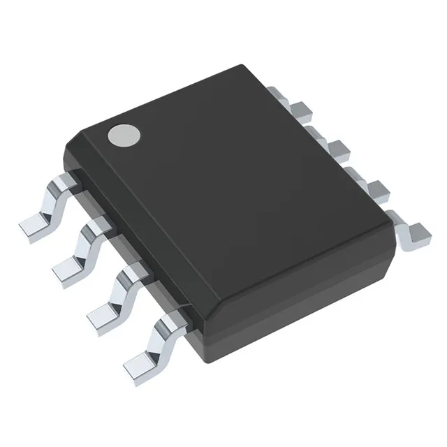
JFET-input dual op-amp for signal conditioning
Each of the two channels can source or sink 10 mA.
For a 1 V peak-to-peak output, the full-power bandwidth is about 2 MHz; above that, slew limiting sets in. This is adequate for audio-band processing (20 Hz–20 kHz) and low-frequency control loops, but insufficient for video or high-speed data acquisition. The JFET input stage keeps bias current at 30 pA, so the TL082ACDR can interface with high-impedance sources (piezo sensors, photodiodes) without loading the signal.
Rated for a total supply span of 10 V to 30 V, the TL082ACDR works on ±5 V to ±15 V split rails or a single 10 V to 30 V rail. Each output can deliver 10 mA — enough to drive a headphone or a standard ADC input, but not a power stage directly.
No exposed thermal pad — junction-to-ambient thermal resistance is handled through the SOIC leads and PCB copper.