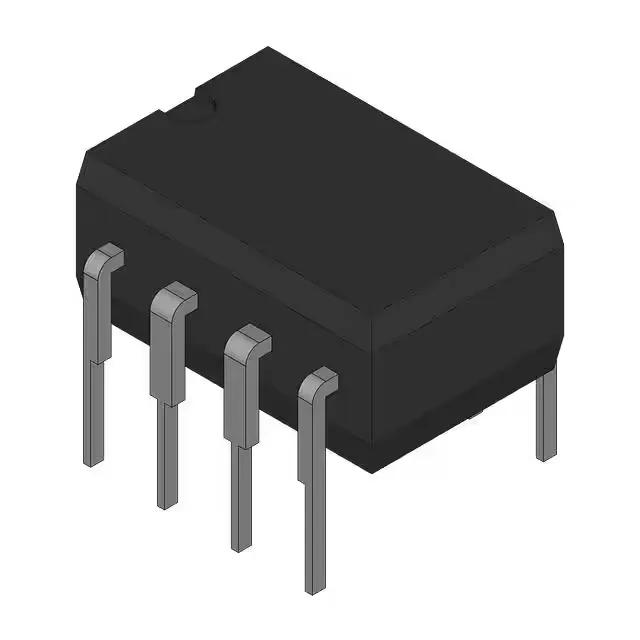
What the 8-DIP package means for your reflow profile
The TL052CP ships in an 8-DIP (0.300", 7.62mm) through-hole package — no reflow profile to worry about, but the wave-solder dwell time and preheat ramp matter. The 8-PDIP body has a 2.54 mm lead pitch, so it sits cleanly in a standard 0.100-inch socket or solders into plated through-holes without tombstoning risk. Moisture sensitivity is not a concern for DIP packages — no bake required before wave soldering, unlike MSL-rated surface-mount parts that popcorn in the oven. The tube packaging keeps leads co-planar and protected from handling damage during kitting.
JFET input stage: what 30 pA bias buys you on the bench
The J-FET input stage draws only 30 pA of input bias current typical — this keeps the voltage error across a 10 kΩ source resistor under 0.3 µV, negligible for precision analog front-ends. Gain-bandwidth product is 3 MHz with a 20.7 V/µs slew rate — the combination sets the large-signal bandwidth ceiling. For a 10 V peak-to-peak output swing, the full-power bandwidth is about 330 kHz (slew rate / (π × Vpp)). Below that, the 3 MHz GBW governs small-signal gain flatness. Each of the two channels draws 4.8 mA supply current, totaling 9.6 mA for the dual package at 30 V maximum supply. The 80 mA per-channel output current drives 600 Ω loads to within a couple volts of the rails — not rail-to-rail, but adequate for driving ADC inputs or moderate cable capacitance.
Active production — no last-time-buy clock ticking
That wide compliance range simplifies power supply design — no need for a dedicated low-noise rail if the system already has ±12 V or ±15 V.