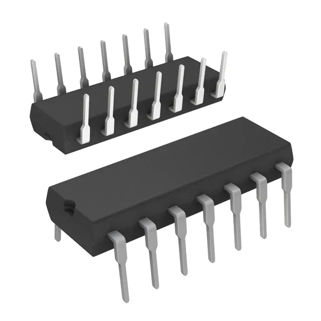
Quad JFET op-amp for commercial-temperature signal chains
The four channels share a total supply current of 870 µA, which keeps the thermal budget low in multi-channel boards running from ±5 V to ±15 V rails (10 V to 30 V total supply span).
The 5.1 V/µs slew rate means the TL034CN can swing a 10 V peak-to-peak output at roughly 80 kHz before slew-rate limiting sets in (full-power bandwidth ≈ slew rate / (π × V_pp)). For smaller signals the 1.1 MHz gain-bandwidth product governs small-signal response: a non-inverting gain-of-10 stage has a closed-loop bandwidth near 110 kHz. If your design needs to pass a 500 kHz square wave cleanly, the 5.1 V/µs figure tells you the edge rate will be the bottleneck, not the GBW.
2 pA input bias and 790 µV offset — the JFET advantage for high-impedance nodes
The 2 pA typical input bias current is the headline reason to pick a JFET op-amp over a bipolar one. In a transimpedance amplifier with a 10 MΩ feedback resistor, 2 pA of bias creates just 20 µV of offset error at the output — negligible. The 790 µV typical input offset voltage is modest for a JFET stage; it will dominate error in DC-coupled high-gain stages unless you null it or AC-couple. The 40 mA per-channel output current gives enough drive for headphones, analog meters, or driving the input of an ADC with a small RC anti-aliasing filter, but not for heavy loads like a relay coil or a 50 Ω transmission line.
14-DIP through-hole — legacy footprint, rework-friendly
The 14-DIP (0.300″ width, 7.62 mm pitch) through-hole package is the classic dual-inline format. It is socket-friendly for prototyping and field-rework, but it occupies more board area than an equivalent SOIC-14 or TSSOP-14. For a production BOM that has already committed to through-hole assembly, the TL034CN drops into existing DIP-14 footprints without a layout change. The tube shipping medium (50 per tube typical for DIP-14) is standard for through-hole lines.