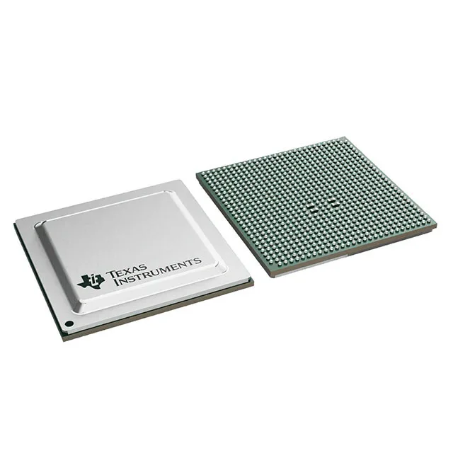
The Texas Instruments TDA4VM88TGBALFR is an automotive-grade heterogeneous system-on-chip (SoC) that combines an ARM Cortex-A72 application processor, ARM Cortex-R5F real-time cores, C66x digital signal processors, and a C7x DSP accelerator. It is designed for advanced driver-assistance systems (ADAS), autonomous driving perception processing, sensor fusion, and central compute gateways where multiple compute domains must share data with deterministic latency.
Compute architecture — what the core mix means for your pipeline
The Cortex-A72 cluster runs at 2 GHz and handles high-level OS and vision processing; the Cortex-R5F cores at 1 GHz manage real-time control loops and sensor interfaces. The C66x DSPs at 1.35 GHz and the C7x DSP at 1 GHz offload signal-processing and neural-network inference. This split lets you partition a perception pipeline: the A72 runs the Linux stack and object tracking, the R5F handles CAN bus and actuator commands, and the DSPs accelerate radar processing or CNN layers without stealing cycles from the application core.
Connectivity and I/O budget
With 226 general-purpose I/O and interfaces including MCAN (CAN-FD), MMC/SD/SDIO, I²C, SPI, UART, and USB, this SoC can aggregate multiple sensor streams and communicate with domain controllers over standard automotive buses. The peripheral set also includes DMA, PWM, and watchdog timers for safety-critical housekeeping.
No immediate LTB risk exists, making it suitable for new designs requiring long-term supply assurance.