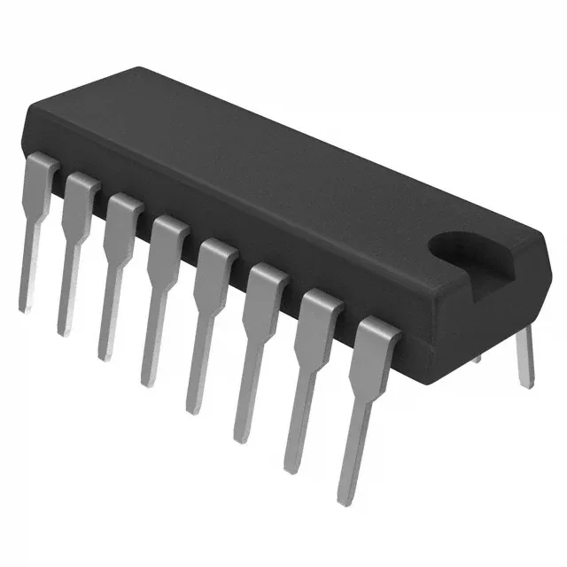
Texas Instruments SN74S175N — Logic ICs

SN74S175N D-Type Flip-Flop, 110 MHz, 16-PDIP

MPNSN74S175N
End of Life

Texas Instruments SN74S175N, 74S series, D-Type flip-flop, 4-bit, positive-edge triggered, complementary outputs, master reset, 110 MHz, 4.75 V to 5.25 V, 16-PDIP, 0°C to 70°C.

$2.99Ref. price · indicative, final on quote
Packaging16-DIP (0.300", 7.62mm)
RoHSROHS3 Compliant
Series74S
Independent supplier — new & surplus stockAuthenticity-screened · ESD-safe packingListing updated Aug 2026

Specifications

SN74S175N specifications
ParameterValue
TypeD-Type
Series74S
Output typeComplementary
Trigger typePositive Edge
MountingThrough Hole
Supply voltage4.75V ~ 5.25V
Current - quiescent96 mA
Current - output high, low1mA, 20mA
Clock frequency110 MHz
Operating temperature0°C ~ 70°C (TA)
PackageTube
FunctionMaster Reset
Case16-DIP (0.300\", 7.62mm)
Number of elements1
Number of bits per element4
Max propagation delay @ v, max CL12ns @ 5V, 15pF

Product details

110 MHz D-type in a 16-pin DIP — what this part is for

The Texas Instruments SN74S175N is a quad D-type flip-flop from the 74S Schottky logic family, clocked at 110 MHz with a propagation delay of 12 ns at 5 V into 15 pF. Each of the four flip-flops shares a common clock and master reset, and outputs are complementary (Q and Q-bar). The 16-pin PDIP package suits through-hole assembly on legacy or low-volume boards where a socketed logic IC is preferred. Typical applications include register storage, shift registers, and synchronous counters in 5 V TTL systems — think industrial controllers, test equipment, or telecom line cards that still run on 74S glue logic.

110 MHz clock and 12 ns propagation — timing budget

The 12 ns max propagation delay (clock to Q, 15 pF load) sets the hold-time margin for the receiving register. The 96 mA quiescent supply current reflects the Schottky clamp speed.

Supply and output drive

The SN74S175N operates from a 4.75 V to 5.25 V supply — a narrow window that assumes a regulated 5 V rail. Output drive is asymmetric: 1 mA source, 20 mA sink. That's enough to drive one or two standard TTL loads directly, but for driving higher fan-out or long backplane traces, buffer the outputs. The complementary outputs give you both polarities without an external inverter, saving board space in counter and register applications.

For dual-sourcing, the SN74LS175NS (surface-mount, 40 MHz, lower power) is a functional alternative if your board can accommodate the slower speed and different package — but it is not pin-compatible in the same socket.

Frequently asked questions

What is the clock frequency and voltage range of SN74S175N?

The SN74S175N clocks at 110 MHz and operates from a 4.75 V to 5.25 V supply. The 12 ns propagation delay at 5 V into 15 pF defines the timing budget for synchronous designs.

What is a suitable replacement for SN74S175N?

The SN74LS175NS (surface-mount, 40 MHz, lower power) is a functional alternative if your design can tolerate the slower clock and different package. For a through-hole drop-in with similar speed, the 74F174PC (80 MHz, 10 ns delay) is a candidate, though it is a 6-bit device with non-inverted outputs only.

What is the function of SN74S175N?

The SN74S175N is a quad D-type flip-flop with master reset and complementary outputs. It stores four bits of data on the positive edge of the clock, and the master reset asynchronously clears all flip-flops.