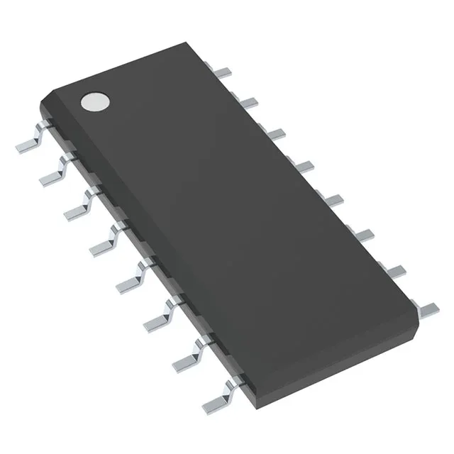
What the 1 x 3:8 configuration means for your address decode
The SN74S138AD is a single 3-line to 8-line decoder/demultiplexer in the 74S Schottky family — the 'S' process gives faster propagation delays than the standard 74LS, which matters when the address lines feed into a memory chip-select tree that must settle within the read cycle window. With one independent circuit decoding three inputs into eight mutually exclusive active-low outputs, it replaces a handful of discrete gates and saves board area when you need to map a 3-bit address space to eight peripheral selects.
Supply rail and output drive — where the numbers hit the board
If your board runs a 3.3 V core and a 5 V I/O rail, the SN74S138AD lives on the 5 V side. Output high current is 400 µA sourced, low current is 8 mA sunk — the asymmetry means the part drives CMOS inputs cleanly but struggles to sink heavy LED loads or relay coils without a buffer.
Temperature grade and package — where this part fits in the enclosure
It does not belong in an unheated outdoor cabinet or under-hood automotive slot; for those you would step to the SN74S138ANSR (industrial-grade sibling) if the rest of the BOM can tolerate the wider temp swing.
Lifecycle and compliance — what the procurement record says
The part carries the standard TI 74S series datasheet with full DC and AC characteristics; the Schottky clamp diodes in the output structure limit undershoot below ground, a detail worth noting if the bus sees long backplane traces with transmission-line reflections.