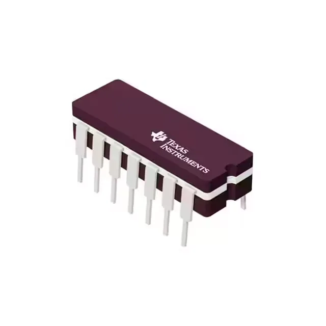
Texas Instruments SN74S02N — Analog & Data Acquisition

SN74S02N 74S NOR Gate, 5V, 14-DIP, Active

MPNSN74S02N
End of Life

Texas Instruments 74S series, Logic Type NOR Gate, 4 Circuits, 2 Inputs, 4.75V ~ 5.25V Supply, Through Hole, 14-DIP (0.300", 7.62mm), 0°C ~ 70°C.

$1.7Ref. price · indicative, final on quote
Packaging14-DIP (0.300", 7.62mm)
StockContact for availability
MOQ1 pcs
  • 100% new & originalTraceable channels only — no refurbs, no pulls, no remarked parts.
  • Date & lot codes on quoteStated per line before you commit; label photos on request.
  • MSL-compliant ESD packingMoisture-sealed bags with indicator cards; reels photo-verified.
  • PayPal buyer protectionPay by T/T, PayPal or Payoneer — card payments covered end to end.

Specifications

SN74S02N Technical Specifications
ParameterValue
Series74S
Logic typeNOR Gate
Mounting typeThrough Hole
Voltage4.75V ~ 5.25V
Current - output high, low1mA, 20mA
Number of inputs2
Operating temperature0°C ~ 70°C
PackageTube
Case14-DIP (0.300\", 7.62mm)
Number of circuits4
Input logic level - low0.8V
Input logic level - high2V
Max propagation delay @ v, max CL5ns @ 5V, 50pF

Product details

74S Schottky NOR gate — still on the active list

The Texas Instruments SN74S02N is a quad 2-input NOR gate from the 74S Schottky logic family, housed in a 14-pin DIP (0.300" body) for through-hole assembly. It runs on a 4.75V to 5.25V supply and is rated over the commercial 0°C to 70°C temperature range. The Schottky-clamped transistors give it a propagation delay of 5 ns at 5V into 50 pF — fast enough for 5V bus timing in older or cost-sensitive digital systems. Each of the four gates can sink 20 mA or source 1 mA at the output, so it drives standard TTL loads directly.

5 ns propagation delay — what it means for the bus

The 5 ns max delay at 5V and 50 pF is the figure that matters for timing closure. In a 5V system clocked at 20 MHz (50 ns period), a single gate eats 5 ns of the budget — fine for a few levels of logic, but you need to count the cumulative delay through a chain. The Schottky process keeps the edge rates clean, so signal-integrity reflections are less of a headache than with slower logic families. The input thresholds are standard TTL: 0.8 V low, 2 V high, so it will interface directly with 74LS, 74ALS, and other 5V TTL families without level translation.

Through-hole DIP — rework-friendly footprint

The 14-DIP package is about as rework-friendly as it gets. No thermal pad to worry about, no hidden balls — just clip the leads, pull the part, and solder in a replacement. The through-hole format also means the part survives a hot-air rework cycle without lifting pads, which matters for repair benches and legacy board rework.

Active lifecycle — no LTB pressure

The SN74S02N carries an Active product status, so there is no last-time-buy deadline or end-of-life notice to manage. It is ROHS3 compliant. For a 74S logic part that has been in production for decades, this means TI continues to manufacture it for the industrial and aftermarket base. You can qualify it into a new BOM without worrying about a sudden obsolescence-driven redesign.

Frequently asked questions

What are the exact electrical specifications for SN74S02N?

The SN74S02N is a quad 2-input NOR gate with a 4.75V to 5.25V supply range. Input logic levels are 0.8 V low and 2 V high. Output current capability is 1 mA high, 20 mA low. Maximum propagation delay is 5 ns at 5V into 50 pF. Operating temperature is 0°C to 70°C.