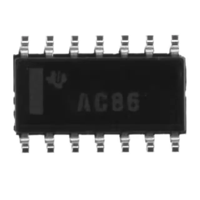
Texas Instruments SN74LVC86ADBR — Analog & Data Acquisition

SN74LVC86ADBR Quad 2-Input XOR Gate, 1.65V-3.6V, 14-SSOP

MPNSN74LVC86ADBR
End of Life

Texas Instruments 74LVC series, SN74LVC86ADBR, XOR (Exclusive OR) gate, 4 circuits, 2-input, 1.65V to 3.6V supply, 24mA output, 4.4ns propagation delay at 3.3V/50pF, -40°C to 125°C, 14-SSOP package.

$0.19059Ref. price · indicative, final on quote
Packaging14-SSOP (0.209", 5.30mm Width)
StockContact for availability
MOQ1 pcs
  • 100% new & originalTraceable channels only — no refurbs, no pulls, no remarked parts.
  • Date & lot codes on quoteStated per line before you commit; label photos on request.
  • MSL-compliant ESD packingMoisture-sealed bags with indicator cards; reels photo-verified.
  • PayPal buyer protectionPay by T/T, PayPal or Payoneer — card payments covered end to end.

Specifications

SN74LVC86ADBR Technical Specifications
ParameterValue
Series74LVC
Logic typeXOR (Exclusive OR)
Mounting typeSurface Mount
Voltage1.65V ~ 3.6V
Current - quiescent1 µA
Current - output high, low24mA, 24mA
Number of inputs2
Operating temperature-40°C ~ 125°C
PackageTape & Reel (TR); Cut Tape (CT)
Case14-SSOP (0.209\", 5.30mm Width)
Number of circuits4
Input logic level - low0.7V ~ 0.8V
Input logic level - high1.7V ~ 2V
Max propagation delay @ v, max CL4.4ns @ 3.3V, 50pF

Product details

Quad 2-input XOR in 14-SSOP — what it does and where it fits

The Texas Instruments SN74LVC86ADBR is a quad 2-input XOR gate from the 74LVC logic family, packaged in a 14-SSOP (5.30 mm width) for surface-mount assembly. It operates from a 1.65 V to 3.6 V supply, with four independent XOR gates each sinking or sourcing 24 mA, and a propagation delay of 4.4 ns at 3.3 V and 50 pF load. The -40°C to 125°C temperature range qualifies it for industrial and automotive under-hood environments.

Supply range and timing — the BOM-fit details

The 1.65 V to 3.6 V supply range means this gate works directly on a 1.8 V FPGA I/O bank or a 3.3 V microcontroller port without extra regulators. The 4.4 ns propagation delay at 3.3 V is fast enough for 50–100 MHz bus-level glue logic; at 1.8 V the delay increases (per the family curve) but remains within a typical 8–10 ns window for slower interfaces like I2C or GPIO expansion. Quiescent current is a maximum of 1 µA, so the static power contribution is negligible even in battery-powered designs that spend most of their time in sleep.

Frequently asked questions

What is the datasheet for SN74LVC86ADBR?

Design engineers need full electrical characteristics, timing diagrams, and application notes to validate the part for their circuit.

What is the pinout of SN74LVC86ADBR?

Engineers must confirm pin assignments for PCB layout and compatibility with existing footprints.

Where can I buy SN74LVC86ADBR?

Sourcing buyers need immediate purchase options and known good distributors to fill BOM lines quickly.

Is SN74LVC86ADBR obsolete?

Brokers and long-term buyers need lifecycle status to avoid supply chain risks or forced redesigns.

What is an equivalent or replacement for SN74LVC86ADBR?

When the exact part is unavailable, finding a drop-in or functional alternative prevents production delays.

What is the price and stock of SN74LVC86ADBR?

Buyers need real-time cost and inventory data to compare suppliers and manage procurement budgets.