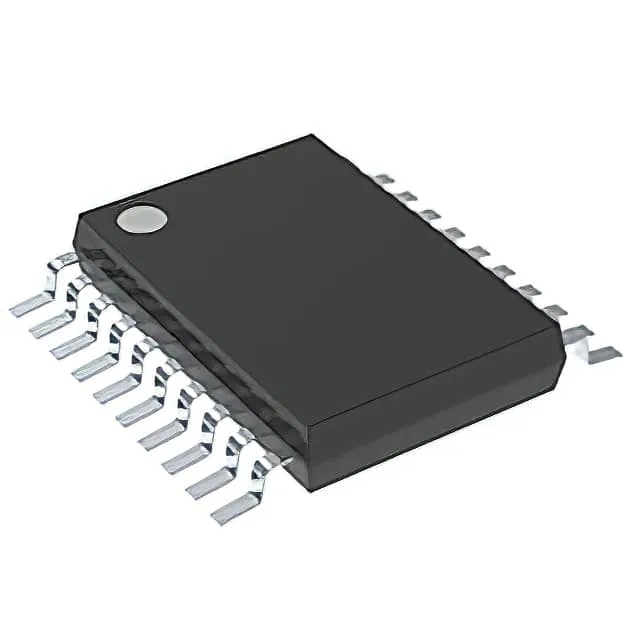
150 MHz clock with 6.8 ns propagation delay
The SN74LVC574APWR clocks at 150 MHz, with a max propagation delay of 6.8 ns at 3.3 V into a 50 pF load. That delay sets the timing budget for the data-to-clock setup window — at 150 MHz the clock period is 6.67 ns, so the 6.8 ns delay means the output transition arrives after the next clock edge. In practice this part is used below its toggle ceiling, where the 6.8 ns figure gives comfortable margin at 100 MHz or slower bus speeds. The 24 mA source and sink drive per output is enough to fan out to eight standard 74LVC inputs without a buffer. The 4 pF input capacitance on the clock line means the upstream driver sees a light load, so the clock edge stays clean.
The 10 µA quiescent current is the standby draw; the dynamic current scales with the toggling rate and the load capacitance, so the power budget is dominated by the output switching, not the bias. The 150 MHz clock spec holds across the full temperature band — no derating curve to worry about for a 100 MHz design.
Active production, no second-source needed
This is a standard-current 74LVC part that TI has been shipping for years and will continue to manufacture — no last-time-buy risk for a design going into production today. The supplier device package confirms the same 20-TSSOP body.