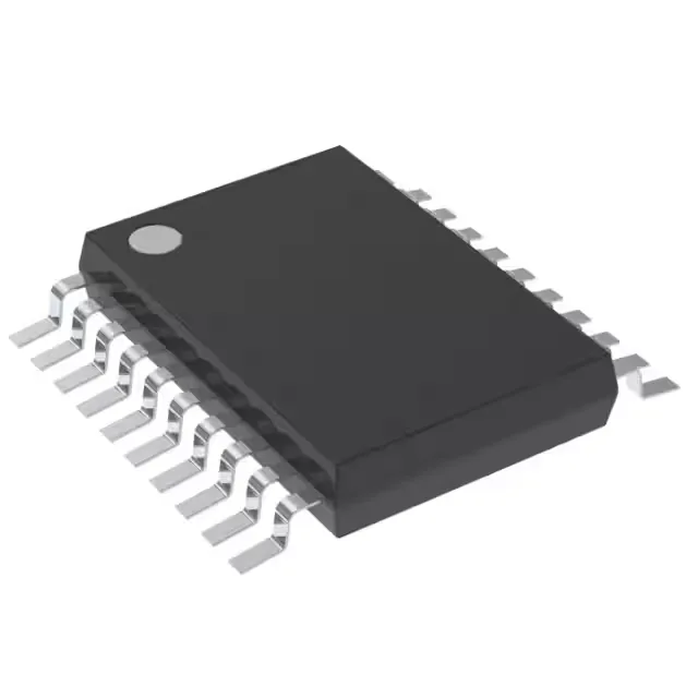
The SN74LVC574ANSR is an 8-bit D-type flip-flop from TI's 74LVC low-voltage CMOS family, clocked at 150 MHz with a positive-edge trigger. It stores one byte of data on each rising clock edge and presents it on tri-state, non-inverted outputs — the standard register for address latching, data buffering, and pipeline stages in mixed-voltage digital systems. Outputs source and sink 24 mA — enough to drive a heavily loaded data bus or a bank of LEDs through a series resistor.
Timing and drive for bus interface design
Maximum propagation delay is 6.8 ns at 3.3 V with a 50 pF load — the spec that sets the data-valid window for the downstream latch. At 150 MHz the clock period is 6.67 ns, so the propagation delay consumes roughly one clock cycle; the designer must budget this into the hold-time margin on the receiving flip-flop. Input capacitance is 4 pF per pin, which matters when the register sits on a shared bus with multiple loads — each additional 74LVC574 adds 4 pF of capacitive load, reducing the bus's maximum toggle rate. Quiescent current is 10 µA typical, negligible in a powered system but relevant for battery-backed domains where the register holds state during sleep.
Industrial temperature grade and package
Housed in a 20-SOIC wide-body package (5.30 mm body width, 0.209-inch pitch), the NSR suffix indicates tape-and-reel or cut-tape delivery. The 20-SO footprint is a standard JEDEC outline; the PCB land pattern matches the common SOIC-20W pad geometry used across the 74LVC and 74AHCT families.
Active lifecycle and compliance
ROHS3 compliant per the manufacturer's declaration, with no exemptions for lead in solder or other restricted substances. No pin-compatible second-source is listed on the manufacturer's cross-reference, but the 74LVC574 function is a standard logic building block with multiple suppliers offering functionally equivalent parts in the same package.