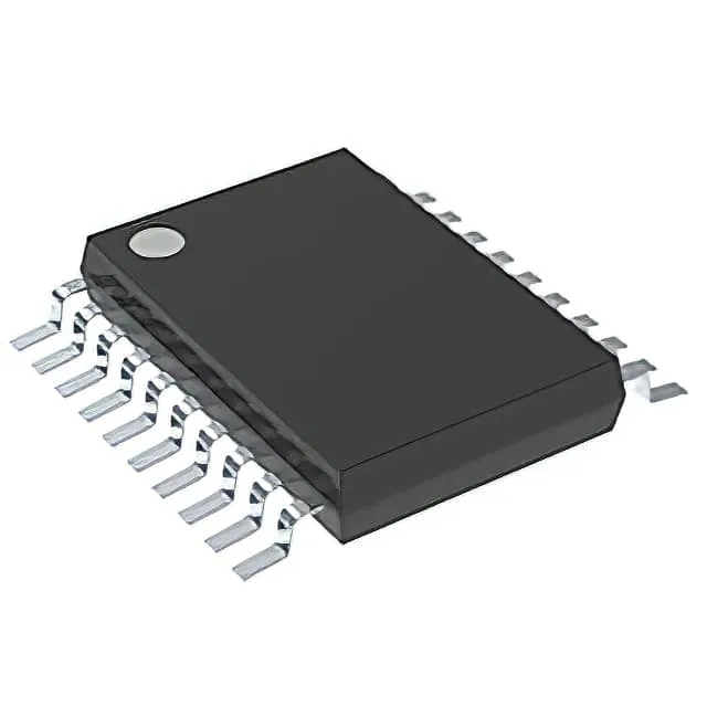
The inverting path and 3-state control let you isolate or invert a data bus with a single device. Each of the eight outputs can sink or source 24mA, enough to drive a bus, a bank of LEDs, or the inputs of a downstream peripheral without an external line driver.
Why the wide supply range matters for your BOM
The 1.65V to 3.6V supply range means one line item covers mixed-voltage boards where a 3.3V bus talks to a 1.8V FPGA bank. You do not need a separate 5V-tolerant buffer or a level shifter — the LVC family was designed for this. If your legacy BOM still uses a 74LS or 74ABT part at 5V, the SN74LVC540APW will not drop in without a supply rail change, but it replaces that function at lower voltage with the same 24mA drive.
It is a current-production device you can qualify into a new design without planning a respin for obsolescence.
20-TSSOP — rework and layout notes
The 20-TSSOP package (4.40mm body width, 0.65mm pitch) is a fine-pitch surface-mount footprint. It is reworkable with hot air if you have a steady hand and a small tip — the leads are exposed and visible, so alignment after reflow is straightforward. The 0.65mm pitch means a standard stencil for 0.5mm or 0.65mm works; just watch the solder paste volume to avoid bridging on adjacent pins.