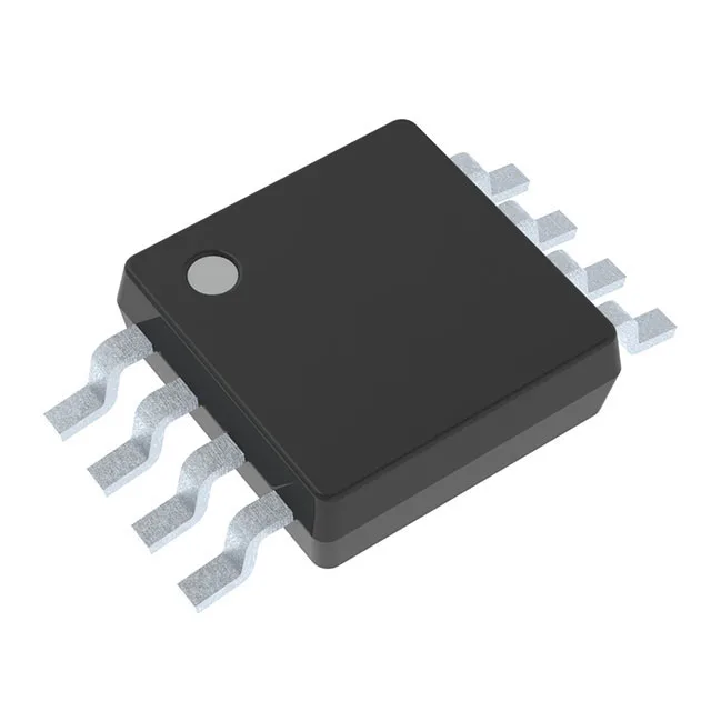
Texas Instruments SN74LVC3G14DCUT — DC-DC Power Modules

SN74LVC3G14DCUT 74LVC Triple Schmitt-Trigger Inverter

MPNSN74LVC3G14DCUT
End of Life

Texas Instruments 74LVC series, SN74LVC3G14DCUT, Inverter Schmitt Trigger, 3 Circuit, 3 Input, 32mA output, 1.65V to 5.5V supply, -40°C to 125°C, 8-VFSOP/8-VSSOP.

$0.9Ref. price · indicative, final on quote
Packaging8-VFSOP (0.091", 2.30mm Width)
StockContact for availability
MOQ1 pcs
  • 100% new & originalTraceable channels only — no refurbs, no pulls, no remarked parts.
  • Date & lot codes on quoteStated per line before you commit; label photos on request.
  • MSL-compliant ESD packingMoisture-sealed bags with indicator cards; reels photo-verified.
  • PayPal buyer protectionPay by T/T, PayPal or Payoneer — card payments covered end to end.

Specifications

SN74LVC3G14DCUT Technical Specifications
ParameterValue
Series74LVC
Logic typeInverter
Mounting typeSurface Mount
Voltage1.65V ~ 5.5V
Current - quiescent10 µA
Current - output high, low32mA, 32mA
Number of inputs3
Operating temperature-40°C ~ 125°C
PackageTape & Reel (TR); Cut Tape (CT)
FeaturesSchmitt Trigger
Case8-VFSOP (0.091\", 2.30mm Width)
Number of circuits3
Input logic level - low0.3V ~ 1.4V
Input logic level - high1.4V ~ 3.7V
Max propagation delay @ v, max CL4.3ns @ 5V, 50pF

Product details

Triple Schmitt-trigger inverter for mixed-voltage signal conditioning

The Texas Instruments SN74LVC3G14DCUT packs three independent Schmitt-trigger inverters into a compact 8-VSSOP package. Its 1.65 V to 5.5 V supply range lets it bridge 1.8 V, 2.5 V, 3.3 V, and 5 V logic domains without a separate level translator — useful when a 3.3 V MCU needs to clean up a 5 V sensor's noisy edge or when a 1.8 V FPGA I/O must drive a 3.3 V peripheral. The Schmitt-trigger inputs add built-in hysteresis, so slow-rising or noisy signals get a clean, jitter-free digital output without external RC filtering. Each of the three channels can source or sink 32 mA, enough to drive an LED indicator or a short PCB trace directly.

4.3 ns propagation delay — timing margin for high-speed paths

With a maximum propagation delay of 4.3 ns at 5 V and 50 pF load, this inverter keeps signal skew tight in clock distribution or deglitching circuits. The 10 µA max quiescent current means it won't eat into a tight power budget when the channels are idle.

Industrial temperature range and active lifecycle

Rated for -40°C to 125°C, the SN74LVC3G14DCUT is a candidate for outdoor telecom cabinets, under-hood automotive modules, and factory-floor I/O. The part carries an Active lifecycle status and is ROHS3 compliant.

Package and footprint: 8-VSSOP

Housed in an 8-VFSOP (0.091", 2.30 mm width) which the supplier device package lists as 8-VSSOP. The fine-pitch, small-body footprint saves board area and is a direct fit for space-constrained designs like handheld instruments or sensor interface modules.

Sourcing and availability

The SN74LVC3G14DCUT is an active, current-production TI part. The part is also available in Cut Tape (CT) for prototyping quantities. For a BOM line that needs this exact triple Schmitt-trigger inverter, the supply channel is open — no allocation drama expected for a standard 74LVC logic part.

Frequently asked questions

What is the propagation delay of SN74LVC3G14DCUT?

At lower supply voltages the delay increases slightly, typical 5–6 ns at 3.3 V.