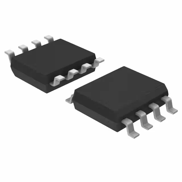
Triple Schmitt inverter — what it does on the board
The Texas Instruments SN74LVC3G14DCTR packs three independent Schmitt-trigger inverters into an SM8 package, each with a single input and a clean inverted output. Each of the three outputs can source or sink 32 mA, enough to drive a standard logic input fan-out of ten or switch a small LED indicator without a buffer. The 4.3 ns max propagation delay at 5 V into a 50 pF load sets the timing budget for the data path — a 50 MHz clock edge through one inverter leaves roughly 20 ns of margin before the next clock edge at 50 MHz, so the path can tolerate two or three series inverters before setup-time closure becomes a concern.
Supply range and quiescent current — power-budget fit
The ROHS3 compliance and active lifecycle status confirm the part ships through the authorized TI distribution chain with full lot traceability and no end-of-life risk for current designs.
Package and footprint — board-fit reality check
The SM8 supplier device package corresponds to the 8-LSSOP / 8-MSOP footprint with a 2.80 mm body width and 0.110-inch (2.80 mm) lead pitch. The surface-mount profile is standard for a small-outline package — a reflow peak of 260°C per JEDEC MSL-1 (typical for TI logic) means no moisture-sensitive bake required if the sealed bag is intact. The 0.50 mm lead pitch demands a standard SMD land pattern; a two-layer board with 0.30 mm traces breaks out all eight pins without a via. The Tape & Reel (TR) and Cut Tape (CT) packaging options suit both high-volume pick-and-place and prototype hand-assembly. The 8-pin MSOP body is small enough for dense layouts but large enough for hand-soldering with a fine-tip iron if the reflow oven is not available — the 0.65 mm lead pitch is forgiving for manual work.