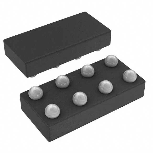
8-DSBGA package and board integration
The SN74LVC2G32YZPR comes in an 8-DSBGA package measuring 1.9x0.9 mm — a wafer-level chip-scale footprint that places the solder balls directly on the die. This means the PCB land pattern must match the ball pitch and diameter exactly; there is no molded body to absorb misalignment. The 0.5 mm typical ball pitch demands a soldermask-defined pad with a via-in-pad only if the via is filled and plated flat, otherwise the ball wicks solder away from the joint. Because the DSBGA has no exposed thermal pad, the primary heat path is through the solder balls into the PCB copper. For a gate drawing 10 µA quiescent and sourcing 32 mA per output, self-heating is negligible — the board copper just needs to handle the I/O trace currents. The 0.9 mm seated height keeps the part low-profile for tight stack-ups.
Supply voltage range and logic-level thresholds
The low-level input threshold sits at 0.7 V to 0.8 V, and the high-level threshold at 1.7 V to 2 V — these are fixed relative to ground, not ratiometric to VCC, so the gate reliably interprets a 1.8 V signal as logic high even when powered from 3.3 V. Propagation delay is 3.2 ns typical at 5 V with a 50 pF load, which keeps the gate transparent in most control and data-path applications below 100 MHz.
Sourced through authorized and independent distribution channels. The 74LVC family is widely second-sourced; if a pin-compatible alternative is needed for a BOM hedge, the standard 8-DSBGA footprint accepts most dual-gate 74LVC parts from TI or competitors with the same package code.