Dual NAND gate with Schmitt-trigger inputs — 5 ns propagation delay at 5 V
The SN74LVC2G132DCTR is a dual 2-input NAND gate from the 74LVC family, integrating Schmitt-trigger inputs on both channels. Maximum propagation delay is 5 ns at 5 V with a 50 pF load — this sets the timing floor for the signal path. The 32 mA symmetric output drive (both high and low) can directly switch small relays, LEDs, or drive multiple CMOS inputs without a buffer. Quiescent current is 10 µA max, so the gate adds negligible standby draw in battery-powered or always-on circuits. The Schmitt-trigger hysteresis on each input cleans up slow edges or noisy signals — the low-level threshold ranges from 0.39 V to 1.87 V depending on supply, and the high-level threshold from 1.16 V to 3.33 V, giving a typical hysteresis window of about 0.8 V at 3.3 V.
Package and board-fit — SM8 (8-LSSOP / 8-MSOP)
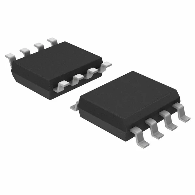
Supplied in an SM8 package, which is the TI designation for an 8-lead LSSOP or MSOP with a 0.110-inch (2.80 mm) body width. The surface-mount footprint is shared across the 74LVC family's small-outline packages — the same land pattern serves the SN74LVC2G08 (AND gate) or SN74LVC2G00 (NAND without Schmitt trigger) if a BOM swap is needed. Available in Tape & Reel (TR) or Cut Tape (CT) for prototyping.
Temperature grade and operating envelope
The gate's switching characteristics are guaranteed across this range, so it fits outdoor telecom, engine-bay electronics, or factory-floor control modules where the ambient sees 105°C on a hot day. ROHS3 compliant — no exemptions for lead in solder or any of the six restricted substances plus DEHP, BBP, DBP, and DIBP phthalates.