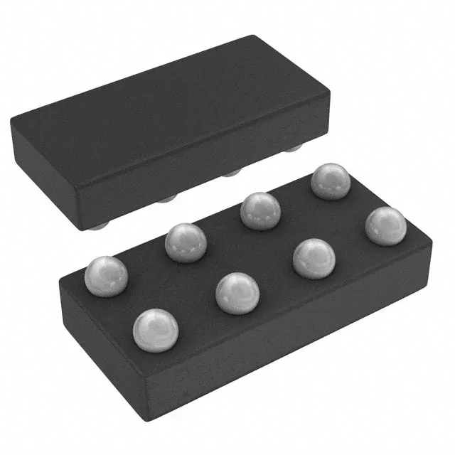
Dual AND gate in a 1.9x0.9 mm BGA
The SN74LVC2G08YZPR packs two independent 2-input AND gates into an 8-bump DSBGA package measuring 1.9x0.9 mm. Each gate delivers 32 mA symmetrical output drive, enough to fan out to multiple CMOS loads or drive a small indicator LED through a current-limiting resistor. Maximum propagation delay is 3.8 ns at 5 V with a 50 pF load, keeping the signal path clean in clock distribution or address decoding up to ~130 MHz.
Input logic thresholds scale with VCC: low at 0.7 V to 0.8 V, high at 1.7 V to 2 V. The 10 µA max quiescent current keeps the idle power draw negligible.
Active production, DSBGA package
It is ROHS3 compliant. The 8-DSBGA package requires a 0.5 mm pitch BGA footprint. Plan for solder-paste stencil aperture of 0.3 mm diameter and X-ray inspection after reflow. Tape & Reel and Cut Tape options are available.