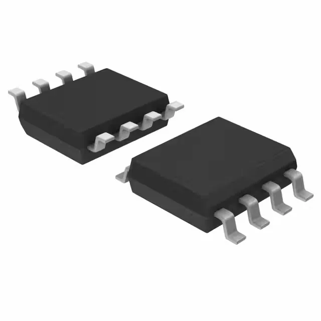
Texas Instruments SN74LVC2G08IDCTRQ1 — Discrete Semiconductors

SN74LVC2G08IDCTRQ1 Texas Instruments AND Gate, AEC-Q100

MPNSN74LVC2G08IDCTRQ1
End of Life

Texas Instruments Automotive AEC-Q100 74LVC series AND gate, SN74LVC2G08IDCTRQ1, dual 2-input, 1.65-5.5V supply, 32mA output, SM8 package, Tape & Reel.

$0.94Ref. price · indicative, final on quote
Packaging8-LSSOP, 8-MSOP (0.110", 2.80mm Width)
StockContact for availability
Lead timeIn Stock wk
MOQ1 pcs
  • 100% new & originalTraceable channels only — no refurbs, no pulls, no remarked parts.
  • Date & lot codes on quoteStated per line before you commit; label photos on request.
  • MSL-compliant ESD packingMoisture-sealed bags with indicator cards; reels photo-verified.
  • PayPal buyer protectionPay by T/T, PayPal or Payoneer — card payments covered end to end.

Specifications

SN74LVC2G08IDCTRQ1 Technical Specifications
ParameterValue
SeriesAutomotive, AEC-Q100, 74LVC
Logic typeAND Gate
Mounting typeSurface Mount
Voltage1.65V ~ 5.5V
Current - quiescent10 µA
Current - output high, low32mA, 32mA
Number of inputs2
Operating temperature-40°C ~ 85°C
PackageTape & Reel (TR); Cut Tape (CT)
Case8-LSSOP, 8-MSOP (0.110\", 2.80mm Width)
Number of circuits2
Input logic level - low0.7V ~ 0.8V
Input logic level - high1.7V ~ 2V
Max propagation delay @ v, max CL3.8ns @ 5V, 50pF

Product details

AEC-Q100 AND gate for mixed-voltage automotive boards

The SN74LVC2G08IDCTRQ1 is a dual 2-input AND gate from the 74LVC family, qualified to AEC-Q100 Grade 3 for automotive applications. It operates across a 1.65 V to 5.5 V supply range, making it suitable for mixed-voltage domains where a 1.8 V MCU core and a 3.3 V peripheral rail share the same bus. Each of the two independent gates delivers 32 mA of output drive in both high and low states, enough to fan out to multiple CMOS loads or drive a small LED indicator without a buffer.

3.8 ns propagation delay at 5 V

Maximum propagation delay is 3.8 ns at 5 V with a 50 pF load. At lower supply voltages the delay increases — at 3.3 V it typically runs around 5 ns, still fast enough for SPI clock rates up to 50 MHz or general-purpose control signals in an automotive ECU. The input logic thresholds track the supply: low-level threshold is 0.7 V to 0.8 V, high-level is 1.7 V to 2 V. This means a 1.8 V logic signal is reliably recognised as high when Vcc is 3.3 V, eliminating the need for a dedicated level translator on the input side.

SM8 package and temperature grade

Housed in an SM8 package (8-lead LSSOP or MSOP with 0.110-inch body width), the part occupies roughly 3 mm × 3 mm of board area. The surface-mount footprint is compatible with standard reflow profiles; no exposed pad or thermal vias are required for the 10 µA quiescent current. Rated for -40°C to 85°C ambient, it covers the passenger cabin and most under-hood auxiliary modules. For 125°C engine-bay locations, the AEC-Q100 Grade 1 variants of the 74LVC family would be the correct choice.

Active lifecycle and compliance

Available in Tape & Reel or Cut Tape options for both prototype and volume assembly. Sourced and quoted to order against your BOM quantity; availability confirmed at RFQ time.

Frequently asked questions

Is SN74LVC2G08IDCTRQ1 a direct drop-in replacement for SN74LVC2G132DCUR?

No. The SN74LVC2G132DCUR is a NAND gate with Schmitt-trigger inputs, while the SN74LVC2G08IDCTRQ1 is a standard AND gate. Both are dual 2-input gates in similar packages, but the logic function differs and the input hysteresis on the 132 variant changes the switching thresholds. A board designed for the 132 will not function correctly with the 08 without a logic-level review.

What compliance documentation does Texas Instruments provide for this part?

Texas Instruments provides ROHS3 compliance certification and a material declaration. The part carries no UL or IEC safety listing — it is a standard CMOS logic IC, not a safety-rated component. AEC-Q100 qualification documentation is available from TI for automotive PPAP submissions.