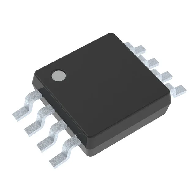
Texas Instruments SN74LVC2G08DCUR — Discrete Semiconductors

SN74LVC2G08DCUR Texas Instruments AND Gate, 1.65V-5.5V

MPNSN74LVC2G08DCUR
End of Life

Texas Instruments 74LVC series AND Gate, SN74LVC2G08DCUR, dual 2-input, 1.65V-5.5V supply, 32mA output, 3.8ns propagation delay, 8-VFSOP package, -40°C to 125°C.

$0.47Ref. price · indicative, final on quote
Packaging8-VFSOP (0.091", 2.30mm Width)
RoHSROHS3 Compliant
Series74LVC
Independent supplier — new & surplus stockAuthenticity-screened · ESD-safe packingListing updated Aug 2026

Specifications

SN74LVC2G08DCUR specifications
ParameterValue
Series74LVC
Logic typeAND Gate
MountingSurface Mount
Supply voltage1.65V ~ 5.5V
Current - quiescent10 µA
Current - output high, low32mA, 32mA
I/O channels2
Operating temperature-40°C ~ 125°C
PackageTape & Reel (TR); Cut Tape (CT)
Case8-VFSOP (0.091\", 2.30mm Width)
Number of circuits2
Input logic level - low0.7V ~ 0.8V
Input logic level - high1.7V ~ 2V
Max propagation delay @ v, max CL3.8ns @ 5V, 50pF

Product details

Supply voltage range and signal-level flexibility

The SN74LVC2G08DCUR: The input logic thresholds track the supply: low-level threshold is 0.7 V to 0.8 V, high-level is 1.7 V to 2 V, so at 3.3 V VCC a 1.8 V logic-high from a low-voltage microcontroller is still recognised as a valid HIGH.

Output drive and propagation delay — timing budget

Each of the two gates can source or sink 32 mA, which is enough to drive a standard LED indicator directly or fan out to four or five CMOS inputs without a buffer. Maximum propagation delay is 3.8 ns at 5 V with a 50 pF load — that 50 pF represents roughly 10 cm of PCB trace plus two or three gate inputs, so the 3.8 ns figure is the realistic ceiling for a typical board-level interconnect, not a bench ideal. Quiescent current tops out at 10 µA across the full supply range, which keeps the static power draw negligible in battery-powered or always-on subsystems.

The 8-VFSOP package (2.30 mm width, 0.091-inch pitch) is a fine-pitch surface-mount footprint that requires standard reflow soldering — the 8-VSSOP supplier device package designation confirms the same body outline for PCB land pattern design.

Frequently asked questions

Will SN74LVC2G08DCUR drop into a board that was specified around SN74LVC2G132DCUR without rewiring?

No — the SN74LVC2G132DCUR is a NAND gate with Schmitt-trigger inputs, while the SN74LVC2G08DCUR is a standard AND gate. Both share the same 8-VFSOP package and supply range, so the footprint is identical, but the logic function differs: a NAND output is the complement of an AND. The board would need a firmware or logic change to account for the inverted output.