Texas Instruments SN74LVC2G07YZPR — Logic ICs

SN74LVC2G07YZPR Dual Buffer, Open Drain, 1.65V–5.5V, 6-DSBGA

MPNSN74LVC2G07YZPR
End of Life

Texas Instruments 74LVC series SN74LVC2G07YZPR, Buffer, Non-Inverting, Open Drain, 1.65V ~ 5.5V, -40°C ~ 125°C, 6-DSBGA.

$2.28Ref. price · indicative, final on quote
Packaging6-XFBGA, DSBGA
RoHSROHS3 Compliant
Series74LVC
Independent supplier — new & surplus stockAuthenticity-screened · ESD-safe packingListing updated Aug 2026

Specifications

SN74LVC2G07YZPR specifications
ParameterValue
Series74LVC
Logic typeBuffer, Non-Inverting
Output typeOpen Drain
MountingSurface Mount
Supply voltage1.65V ~ 5.5V
Current - output high, low-, 32mA
Operating temperature-40°C ~ 125°C (TA)
PackageTape & Reel (TR); Cut Tape (CT)
Case6-XFBGA, DSBGA
Number of elements2
Number of bits per element1

Product details

Dual open-drain buffer in a 0.4mm-pitch BGA

Each of the two elements sinks up to 32mA, enough for an LED, a relay coil, or a bus pull-down. The 6-DSBGA package (0.4mm pitch) saves board area but demands a decent reflow profile and a clean stencil — the scorch mark on a dead board from a poorly soldered BGA is unmistakable.

The 1.65V to 5.5V supply range covers 1.8V, 2.5V, 3.3V, and 5V rails without a level shifter — just pick the pull-up voltage on the open-drain output. At the low end, 1.65V is enough for a 1.8V I/O bank; at 5.5V you can drive a legacy 5V TTL bus. If you're reworking a board that ran hot, this part won't be the first thing to drift.

Open-drain output — the real reason you pick this part

Open-drain outputs let multiple devices share a pull-up resistor — common for interrupt lines, I²C-style buses, or fault flags. The 32mA sink current handles a typical LED with a series resistor, or a 5V relay coil through a transistor driver. There's no internal pull-up, so the high-level voltage is whatever you connect the external resistor to — handy for level translation. Just remember: the output can only pull low; the pull-up resistor and load determine the rise time.

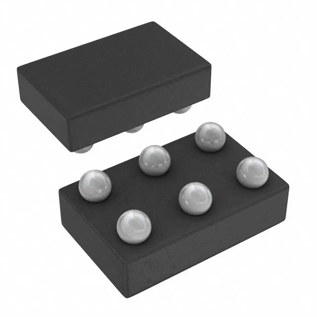
The 6-DSBGA package is a 0.4mm-pitch wafer-level chip-scale package — about 1.0mm × 1.4mm. No leads, no exposed pad; the solder balls are the only connection. Reflow profile needs a peak temperature around 260°C (lead-free), and the board layout must match the TI-recommended footprint exactly. A hot-air rework station can remove it, but the tiny balls make alignment finicky; a stencil and paste are safer.

It's ROHS3 compliant.

Frequently asked questions

Is SN74LVC2G07YZPR a replacement for SN74LVC2G06?

The SN74LVC2G06 is also a dual inverter with open-drain outputs, but it's an inverting buffer (the '06 suffix). The SN74LVC2G07 is non-inverting. They are pin-compatible in the same package, but the logic function differs — check your design's polarity before swapping.

Is SN74LVC2G07YZPR RoHS compliant?

Yes, it is ROHS3 Compliant.

Are there any alternatives to SN74LVC2G07YZPR?

A close functional alternative is the SN74LVC2G17QDCKRQ1, which is also a dual non-inverting buffer but with Schmitt-trigger inputs and push-pull outputs — not open-drain. The SN74LVC2G07's open-drain output is the key difference; if you need a wired-OR or level-shifting capability, the '07 is the right choice. For a pin-compatible open-drain alternative, check the SN74LVC2G06 (inverting) in the same DSBGA package.