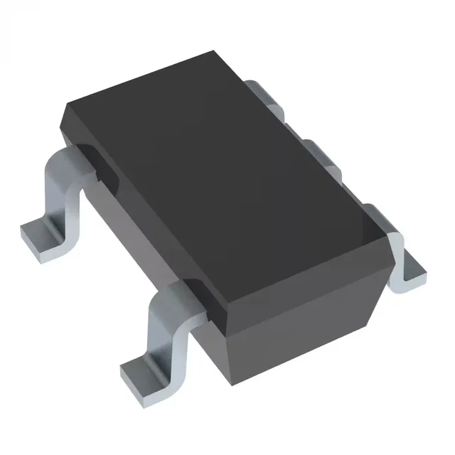
Single unbuffered inverter for mixed-voltage glue logic
The SN74LVC1GU04DBVR: Supply range is 1.65V to 5.5V. The unbuffered output stage gives a linear transfer characteristic. Symmetric output drive of 32mA source and sink at 3.3V handles moderate capacitive loads and multiple fan-out to downstream gates. Propagation delay is 3.5ns typical at 5V with a 50pF load, fast enough for most 10-20 MHz clock distribution or control signal inversion.
3.5ns propagation delay — timing budget for the bus
The 3.5ns max propagation delay at 5V and 50pF load is the number to check against your timing closure. At 3.3V the delay will be slightly higher, typically around 4.5ns. For a 20 MHz clock path that gives roughly 10ns of period, leaving 6.5ns of margin after the inverter delay — adequate for most board-level glue. If you are running at 50 MHz or above, budget the delay into the signal-integrity simulation rather than assuming it vanishes. Quiescent current maxes at 10 µA, negligible for battery-powered designs. The 32mA output drive is symmetric, so rise and fall times match closely — helpful for maintaining duty cycle in clock inversion paths.
There is no end-of-life notification, no last-time-buy window to track. ROHS3 compliant per the listing, so it passes EU and California regulatory requirements without an exemption.
SOT-23-5 footprint and supply routing
The SOT-23-5 package is a five-pin small-outline transistor package. Minimum supply is 1.65V.