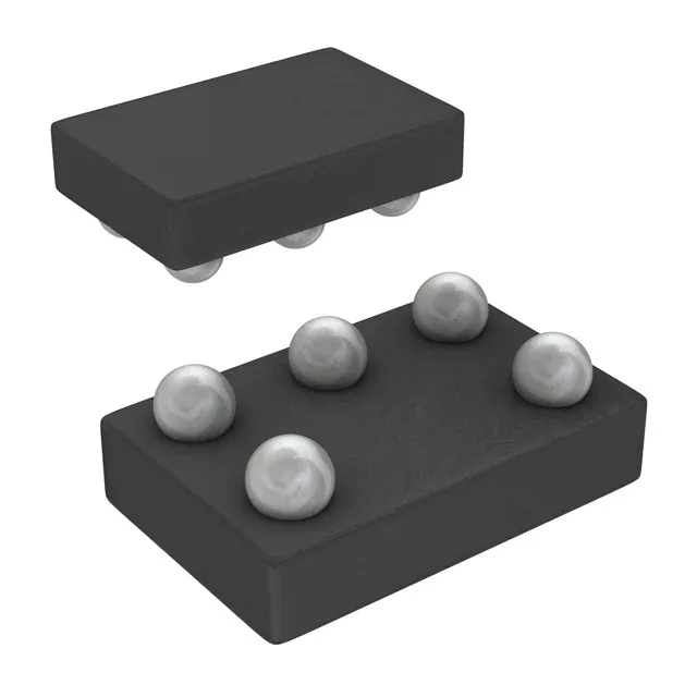
Single-gate XOR in 5-DSBGA — what the package means for your board
It packs one gate into a 5-bump DSBGA (1.4 mm × 0.9 mm) — the kind of footprint that saves board area on a smartphone mainboard or a compact sensor module but demands a capable pick-and-place and a reflow profile tuned for the 0.5 mm ball pitch. Output drive is rated 32 mA per pin, symmetric sink and source, which is enough to directly drive a low-power LED or feed a downstream CMOS input without a buffer. Quiescent current maxes at 10 µA, so it won't eat into a battery budget. Propagation delay clocks in at 4 ns typical with a 5 V supply and 50 pF load — fast enough for most glueless interface logic, level translation, or parity checking at moderate clock rates.
DSBGA rework and soldering — what the repair tech needs
There is no exposed side leads — all connections are under the body. That means visual inspection of solder joints requires X-ray. For rework, a hot-air station with a fine nozzle (3–4 mm diameter) and a profile peaking around 260 °C works; prebake at 125 °C for 8 hours if the moisture-barrier bag has been open past the floor-life window. Stencil aperture for the 0.5 mm pitch should be 1:1 with the pad, and the PCB land pattern should follow TI's recommended footprint — no via-in-pad unless filled and plated.
Sourcing — active, ROHS3, and available to quote
Submit an RFQ for your target quantity and we'll respond with a firm offer.