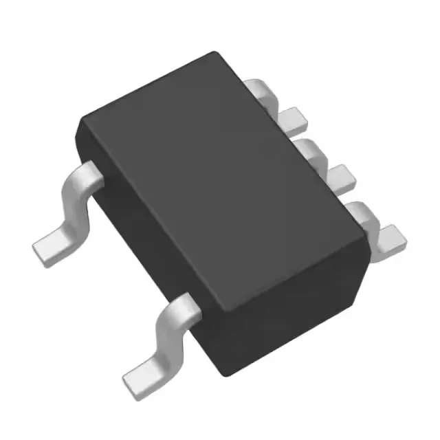
Single-bit D-type flip-flop for high-speed bus isolation
It stores one data bit and presents a non-inverted output on the rising edge of the clock. Clock frequency is rated at 160 MHz, with a maximum propagation delay of 4.5 ns at 5 V into a 50 pF load. Output drive capability is ±32 mA, enough to feed a standard CMOS input or drive a small LED without an external buffer. Quiescent current is 10 µA, keeping the standing power low in battery-powered equipment. The SC-70-5 package (2.0 mm × 2.1 mm body) fits into dense PCB layouts where board area is at a premium.
Supply voltage range and mixed-voltage interface
One flip-flop variant can serve as a level translator between a 1.8 V microcontroller GPIO and a 3.3 V sensor, or between a 3.3 V FPGA and a 5 V legacy backplane. The input thresholds track VCC, so at 1.8 V the VIH is about 1.26 V; at 5 V it is 3.5 V. Input capacitance is 4 pF, which keeps the loading light on the driving node even when multiple flip-flops are paralleled on a shared clock line. The positive-edge trigger simplifies timing analysis because the setup and hold windows are referenced to the rising edge only.
Propagation delay and timing closure
The 4.5 ns max propagation delay at 5 V is the number to budget for worst-case timing. If the clock-to-Q delay of the driving flip-flop is 3 ns and the SN74LVC1G79DCKT adds 4.5 ns, the receiving register must have a setup time greater than 7.5 ns to avoid a metastability window. At 160 MHz the clock period is 6.25 ns, so this part is best used in one- or two-gate delay paths rather than deep pipelines at full frequency. For lower-speed clocks the margin is generous.
Package and footprint for dense layouts
The SC-70-5 package (also known as SOT-353) has a 2.0 mm × 2.1 mm footprint with 0.65 mm pin pitch. It is one of the smallest packages for a single-gate logic function. The five pins are VCC, GND, D, CLK, and Q. The small body means the decoupling capacitor must be placed close — a 0.1 µF ceramic in 0402 or 0201 size fits directly adjacent. No thermal pad is needed; the package dissipates through the leads and the small epoxy body.
ROHS3 compliance is confirmed.