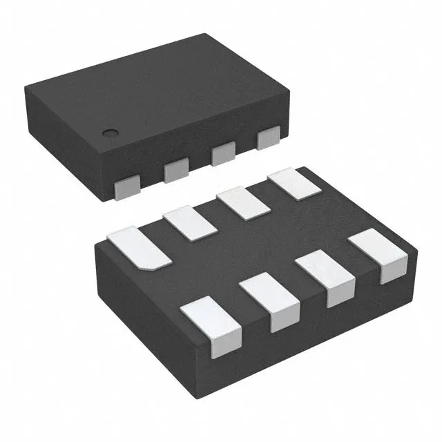
Single-bit D-type with set and reset — 200 MHz in a 1.4x1 mm package
It includes both Set (Preset) and Reset inputs, and provides complementary Q and Q̅ outputs. Clock frequency reaches 200 MHz, and the output can source or sink 32 mA symmetrically. Propagation delay is 4.4 ns at 5 V with a 50 pF load. The device is housed in an 8-X2SON package measuring 1.4 x 1.0 mm, suited for dense PCB layouts in portable and industrial equipment.
Supply voltage flexibility and temperature range
Quiescent current is 10 µA typical, which is negligible in most applications but worth noting for battery-powered designs that spend long periods in idle.
Output drive and timing margin
Symmetric 32 mA output drive at both high and low levels means the part can drive a 50 pF load with a 4.4 ns propagation delay at 5 V. This drive strength is sufficient for clock distribution to multiple loads or for driving short PCB traces without a buffer. At lower supply voltages (e.g., 1.8 V), the propagation delay will increase — the 4.4 ns figure is at 5 V, so budget additional margin when operating at 3.3 V or 1.8 V. Input capacitance is 5 pF, which is low enough to not load the driving gate significantly at 200 MHz.
The 8-X2SON package (1.4 x 1.0 mm body, 0.5 mm pitch) is a leadless package with exposed pads underneath. It requires a solder-paste stencil designed for the specific land pattern — the datasheet's recommended footprint should be followed exactly. Reflow profile must match the solder paste specification; the small thermal mass means the package reaches peak temperature quickly.