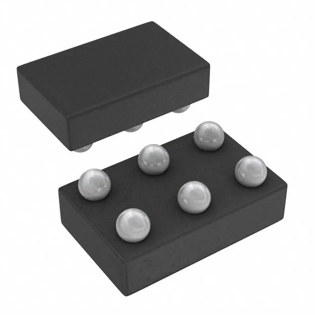
Single 3-input OR gate in a tiny DSBGA package
3.5 ns propagation delay — timing headroom at 5 V
Maximum propagation delay is 3.5 ns at 5 V with a 50 pF load.
The low-level input threshold sits at 0.7 V to 0.8 V, and the high-level threshold at 1.7 V to 2 V, so it cleanly recognizes 1.8 V logic as a high without needing external level shifters. The 10 µA maximum quiescent current is negligible for battery-powered designs.
The 6-DSBGA package (0.9 mm x 1.4 mm typical) saves significant board area compared to a SOT-23 or SC-70, but it is a leadless BGA-style package. The solder balls are under the device, so you need a solder-paste stencil with small apertures and X-ray inspection to verify joint integrity.