Qualified for the underhood, sized for the tight spot
That means it is not an industrial part being marketed as 'automotive-capable' — it carries the grade documentation an OEM auditor expects to see in a PPAP package. Output drive is 32 mA per pin, enough to switch a small relay coil or drive a signal through a long harness segment. The propagation delay of 4.5 ns at 5 V and 50 pF keeps it in budget for CAN transceiver enable signals and sensor interrupt paths running at a few MHz.
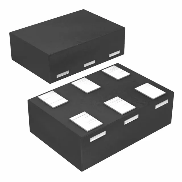
Package reality: 6-UFDFN, not a through-hole part
This is a surface-mount device in a 6-UFDFN package (the supplier device package is 6-SON, 1.45 mm x 1.0 mm per the base number family). That footprint is tiny — about the size of a 0402 resistor — so the PCB layout needs a well-defined solder-paste aperture and a stencil design that does not bridge the narrow pitch. There is no exposed thermal pad to worry about; the quiescent current is only 10 µA max, so self-heating is negligible even at 125°C ambient.
That makes it a safe choice for a new BOM line that will run for several years. There is no risk of a sudden discontinuation mid-program.
What the 4.5 ns propagation delay means for your bus
The 4.5 ns figure is specified at 5 V supply and 50 pF load, which is a standard test condition. In a real 3.3 V system with a 15 pF gate load (one or two downstream inputs), the delay will be shorter — typically in the 2.5 ns to 3.5 ns range. If you are clocking a signal at 10 MHz or higher, budget the delay against the set-up time of the receiving flip-flop; the 74LVC family has tight output-edge rates that help keep the timing margin healthy.