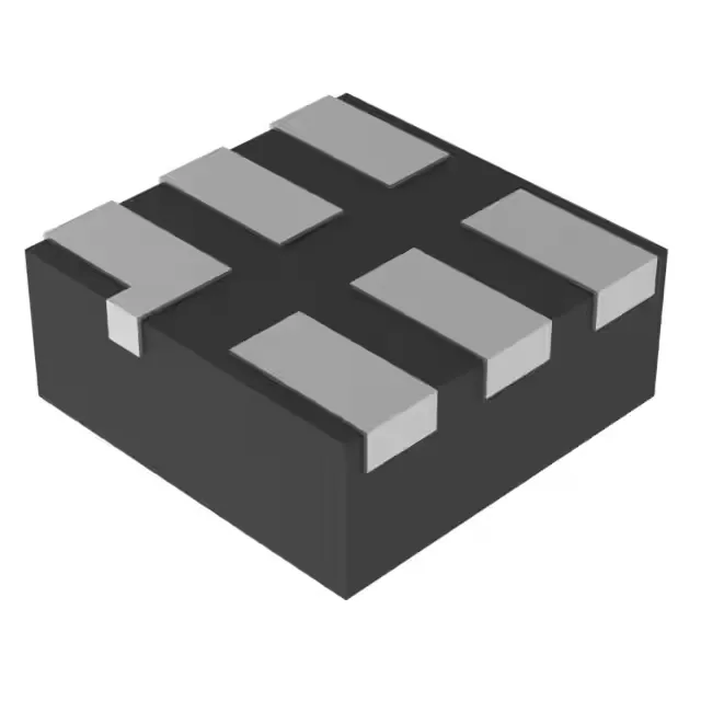
Single OR gate in a 1 mm² SON package
The device is housed in a 6-XFDFN (6-SON) package measuring just 1x1 mm, suited for wearable, IoT, and portable electronics where every square millimeter counts.
A designer can place this part in an engine-bay ECU or a rooftop base station without derating concerns.
Output drive and switching speed
Symmetric 32 mA output drive on both high and low levels is generous for a single-gate device. It can directly switch a small LED indicator or fan out to several CMOS logic inputs without an external buffer. The maximum propagation delay of 4 ns at 5 V with a 50 pF load keeps the gate fast enough for most 50 MHz clocked buses and control signals. At lower supply voltages the delay increases, but the 74LVC family maintains consistent performance across the range.
No last-time-buy or obsolescence risk applies to this part at this time.
Package and PCB integration
The 6-XFDFN (6-SON) package with a 1x1 mm body is a leadless, very thin package. The supplier device package is 6-SON (1x1). This footprint requires a fine-pitch stencil and careful solder-paste volume control to avoid bridging. The exposed pad (if present) is not a thermal pad but a tie to the substrate; verify the land pattern from the TI application note for this package.