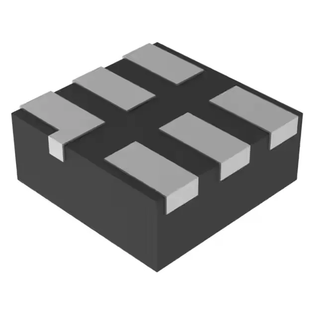
Single-channel bus buffer in a 1x1 mm SON
The Texas Instruments SN74LVC1G125DSFR is a single-bit, non-inverting buffer with a 3-state output, part of the 74LVC logic family. It operates from 1.65 V to 5.5 V, making it suitable for mixed-voltage systems where a 1.8 V core talks to a 3.3 V peripheral. The 32 mA symmetrical output drive handles standard bus loads without external line drivers.
The supply voltage spans the full 1.65 V to 5.5 V range, covering common logic rails from 1.8 V through 5 V. The 3-state output lets multiple devices share a bus line — pull the output enable low and the output goes high-impedance, releasing the bus.
32 mA drive — enough for a loaded bus
Both the high and low output current are rated at 32 mA, which is typical for the 74LVC family. That drive strength can handle a fan-out of ten standard LSTTL loads or drive a short cable stub. If your bus has more than a dozen loads or runs longer than a few inches, budget for the voltage drop across the trace resistance — the output impedance is low enough that a 50 Ω trace will see a clean edge, but the DC drop at 32 mA through a 0.5 Ω trace is only 16 mV, negligible.
The 74LVC process holds timing over the full range; expect propagation delay to shift by about 30% from 25°C to 85°C, which is within the datasheet limits. For under-hood or engine-bay use, you would need an AEC-Q100 qualified variant like the SN74LVC2G17QDCKRQ1.
6-SON (1x1 mm) — layout checklist
The 6-SON package (also called 6-XFDFN) has a 1x1 mm body with a 0.5 mm pitch. Route a via under the pad to the ground plane; the datasheet recommends a 0.3 mm via with a 0.5 mm capture pad. The small footprint means the decoupling cap must sit within 2 mm of the supply pin — a 0.1 µF ceramic in a 0402 or 0201 case fits alongside.