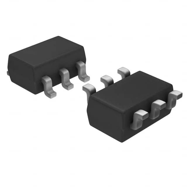
Texas Instruments SN74LVC1G11DBVR — Logic ICs

SN74LVC1G11DBVR AND Gate, 1.65V-5.5V, SOT-23-6

MPNSN74LVC1G11DBVR
Active

Texas Instruments 74LVC series single 3-input AND gate, SN74LVC1G11DBVR, 1.65V to 5.5V supply, 32mA output, 3.5ns propagation delay, -40°C to 125°C, SOT-23-6 package.

$0.4100Ref. price · indicative, final on quote
PackagingSOT-23-6
RoHSROHS3 Compliant
Series74LVC
Independent supplier — new & surplus stockAuthenticity-screened · ESD-safe packingListing updated Aug 2026

Specifications

SN74LVC1G11DBVR specifications
ParameterValue
Series74LVC
Logic typeAND Gate
MountingSurface Mount
Supply voltage1.65V ~ 5.5V
Current - quiescent10 µA
Current - output high, low32mA, 32mA
I/O channels3
Operating temperature-40°C~125°C
PackageTape & Reel (TR); Cut Tape (CT)
CaseSOT-23-6
Number of circuits1
Input logic level - low0.7V ~ 0.8V
Input logic level - high1.7V ~ 2V
Max propagation delay @ v, max CL3.5ns @ 5V, 50pF

Product details

Its supply range of 1.65V to 5.5V means it can sit on a 1.8V, 2.5V, 3.3V, or 5V rail without a level translator, which is exactly what you want when stitching together a multi-voltage board. The 3.5ns propagation delay at 5V with a 50pF load keeps timing closure manageable in fast paths, though at lower supply voltages the delay stretches — budget for it if your design runs at 1.8V and the signal chain has tight cycle-to-cycle requirements. The 10 µA max quiescent current means it won't eat into a sleep-mode budget.

No special handling for lead-free reflow profiles beyond the standard MSL precautions for SOT-23-6.

SOT-23-6 footprint — what to watch on layout

The SOT-23-6 package (supplier device package SOT-23-6, case code SOT-23-6) is a common small-outline transistor package. The 0.95 mm pin pitch is standard, but the narrow body means the pad layout needs to match the TI recommended land pattern — a generic SOT-23-6 footprint from a library may have oversized pads that create solder-bridge risk on the tight pin spacing.

Frequently asked questions

Is SN74LVC1G11DBVR compatible with 5V logic?

Yes. The supply voltage range of 1.65V to 5.5V means it operates directly on a 5V rail. The input logic levels are specified as 1.7V to 2V for a logic high and 0.7V to 0.8V for a logic low, which are compatible with standard 5V CMOS and TTL thresholds across the full supply range.

What is the difference between SN74LVC1G11DBVR and SN74LVC1G11DCKR?

Both are the same die — a single 3-input AND gate from the 74LVC family — but they differ in package and tape/reel format. The DCKR suffix typically indicates a different package variant (SC-70-6). The electrical specs (supply range, drive current, propagation delay, temperature range) are identical; the choice is purely a footprint and handling decision.