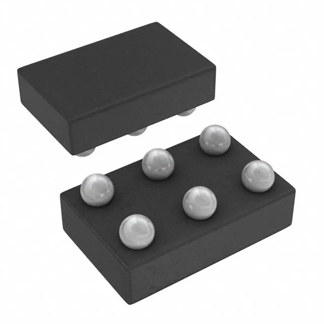
Single 3-input NAND gate in a 0.4mm-pitch BGA
The gate delivers 32 mA source and 32 mA sink output current, enough to drive an LED or a short PCB trace directly. Propagation delay is 3.6 ns at 5 V with a 50 pF load, which keeps signal integrity clean in clock distribution and control logic paths running at moderate speeds.
Quiescent current is 10 µA max, so it adds negligible draw in battery-backed or always-on sections.
Package reality: 6-DSBGA layout considerations
The 6-DSBGA (0.4 mm ball pitch) is the smallest footprint for a single-gate NAND — about 1.3 mm² board area. That saves space but demands a fine-pitch PCB process (≥0.2 mm trace/space) and a solder-mask-defined pad. The supplier device package is 6-DSBGA; there is no larger SOIC or TSSOP alternative for this order code. If your assembly line cannot handle 0.4 mm pitch BGA, look at the SN74LVC1G10DCKR (SC-70) or SN74LVC1G10DBVR (SOT-23-5) — same logic function, larger leaded packages.
The base product number is 74LVC1G10, and the 74LVC series remains a mainstream logic family with broad second-source availability from Nexperia, NXP, and ON Semiconductor. For dual-sourcing, the SN74LVC1G10DBVR (SOT-23-5) and SN74LVC1G10DCKR (SC-70) are pin-compatible functional equivalents in leaded packages, though not identical BGA footprint.