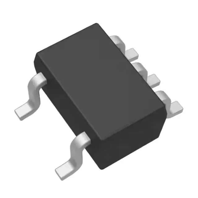
What this single AND gate does in a board
It performs the basic AND logic function on two inputs and outputs a single result. Typical applications include signal gating, enable/disable logic, and general-purpose glue logic in industrial controls, telecom modules, and portable electronics where board area is tight.
It means this gate can live on a 1.8 V FPGA bank, a 3.3 V MCU rail, or a 5 V legacy bus without a separate regulator. If you need to fan out to more than a few loads or drive a long backplane trace, budget a buffer after this gate.
4 ns propagation delay — timing budget check
In a 100 MHz clock path or a critical setup/hold window, you need to verify that 4 ns plus the interconnect delay stays within your timing margin. At lower supply voltages the delay increases — at 3.3 V expect roughly 5–6 ns, and at 1.8 V around 8–10 ns. If your path is timing-critical, simulate with the actual load and supply.
Package and footprint — SC-70-5
The SC-70-5 (also known as SOT-353) is a 5-lead package with 0.65 mm pitch. It is one of the smallest packages for a single gate, making it a fit for dense PCBs where every square millimetre counts. The supplier device package is SC-70-5. The part is also available in cut tape for prototyping or tape and reel for production. The mounting type is surface mount.
It is ROHS3 compliant.