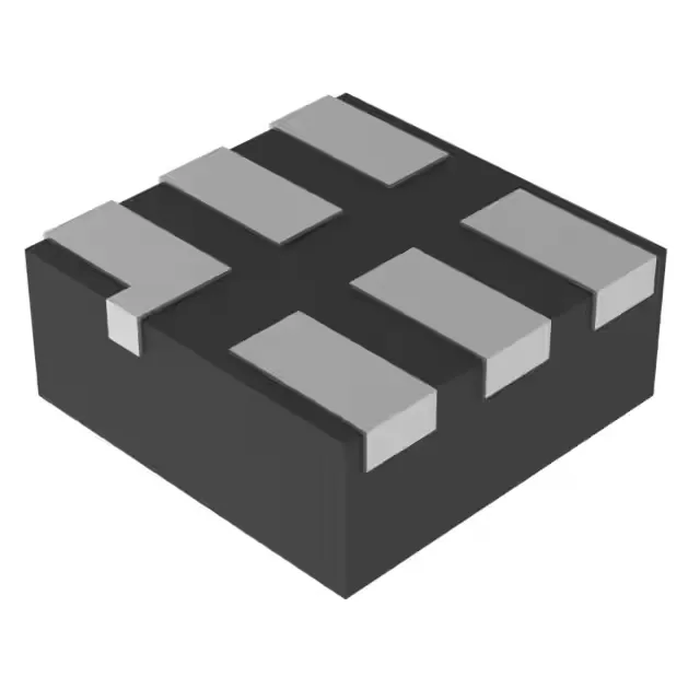
Single-gate inverter in a 1x1 mm SON package
It accepts a supply voltage from 1.65V to 5.5V, making it a natural level translator between 1.8V and 3.3V or 5V logic domains. The output can source or sink 32 mA on each edge, and the propagation delay sits at 3.7 ns with a 5V supply driving a 50 pF load.
3.7 ns propagation delay — timing budget for the signal path
The 3.7 ns max propagation delay at 5V and 50 pF load is the spec that defines this inverter's place in a clock or data path. At lower supply voltages the delay increases — expect roughly 6 ns at 3.3V and closer to 10 ns at 1.8V, following the typical 74LVC derating curve. If your signal chain has tight timing closure at the receiving flip-flop, budget this delay plus the input-to-output rise time. The 32 mA output drive is generous for a single-gate device; it can cleanly drive a short PCB trace or a single fan-out without needing a buffer.
Run it at 1.8V to interface with a low-voltage sensor or FPGA bank, or at 3.3V or 5V for standard TTL/CMOS logic. The input logic levels are specified as 0.7V to 0.8V for low and 1.7V to 2V for high, which means the input threshold shifts with the supply rail. At 3.3V VCC, a 1.8V logic-high from a neighbouring device is still above the 2V high threshold — but at 5V VCC, that same 1.8V signal will not be recognised as a high. Plan the supply voltage against the driving device's output levels.
6-XFDFN (1x1 mm) — footprint and assembly notes
The 6-XFDFN package (also called 6-SON, 1x1 mm) is an ultra-small, leadless package with no visible leads. The pad layout is a 1x1 mm square with six land pads on the bottom. This package is suited for reflow soldering only — no hand-soldering with an iron. The small size means the PCB footprint must be precise; a 0.1 mm offset in the stencil aperture can cause solder bridging between adjacent pads.