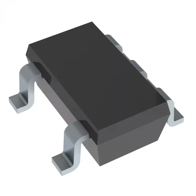
Single-gate inverter in SOT-23-5 — the scorch-mark tells you
The output sinks and sources 32 mA symmetrically, so you can drive a small LED or a relay coil directly without a buffer transistor. Propagation delay is 3.7 ns at 5 V with a 50 pF load, which keeps it in the running for clock inversion or high-speed data-path cleanup.
Supply voltage range — why it matters for a repair bench
When you're tracing a dead rail on a controller board and find a 1.8 V domain talking to a 3.3 V domain, a single-gate inverter from the 74LVC family can level-shift and invert in one package. The 1.65 V lower limit means it works with the latest low-voltage sensors and FPGAs, while the 5.5 V ceiling lets it interface with legacy 5 V logic without a separate translator.
Output drive and timing — what the 32 mA and 3.7 ns actually mean
The 32 mA symmetric output drive is unusual for a single-gate logic part in this package. It means you can directly drive a small LED indicator, a piezo buzzer, or a relay coil without adding a discrete MOSFET or transistor. The 3.7 ns propagation delay at 5 V is fast enough for most clock and data inversion tasks up to about 100 MHz — beyond that, you'd want a dedicated LVCMOS buffer or a faster logic family like AUP.