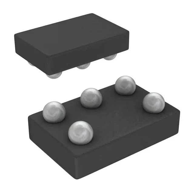
Single NOR gate in a 0.9 mm pitch BGA
Input thresholds track the supply: low at 0.7 V to 0.8 V, high at 1.7 V to 2 V, which means a 3.3 V logic output cleanly drives the high input at 5 V supply, and a 1.8 V MCU pin still meets the low threshold at 1.65 V rail. Output drive is symmetric at 32 mA source and sink, enough to light an LED directly or drive a short trace to another gate input. Quiescent current maxes at 10 µA, so it won't kill a battery budget in sleep mode.
Maximum propagation delay is 4 ns at 5 V with a 50 pF load. That's fast enough for most glue-logic paths in a 48 MHz SPI or a 100 MHz memory interface, as long as the trace length stays under a few inches. At 3.3 V the delay stretches a bit (typical 5 ns range), so budget an extra nanosecond if the design runs at the low end of the supply range.
5-DSBGA: tiny footprint, tight rework window
The 5-DSBGA package measures 1.4x0.9 mm with a 0.5 mm ball pitch. That's a 5-ball array — two on one side, three on the other — so the footprint is about the size of a 0402 resistor. Layout needs a micro-via or a via-in-pad if you route out on a two-layer board; four-layer with ground plane makes it easier. The DSBGA is a wafer-level package, so the balls are the die itself — no mold compound. That means MSL 1 out of the bag, but the balls are delicate: no vacuum pick with excessive force, and rework with hot air requires a preheat to avoid thermal shock. A stencil with 0.25 mm apertures and 0.125 mm thickness works for solder paste.