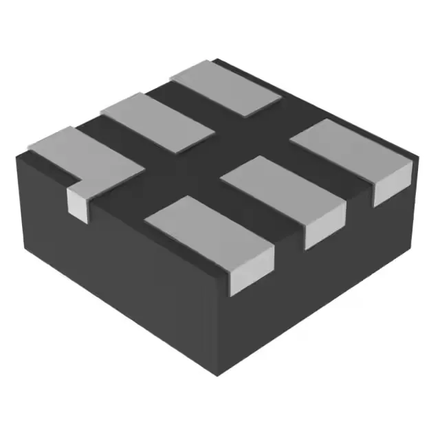
Single-gate NAND in a 1×1 mm package
It operates from 1.65V to 5.5V, making it suitable for mixed-voltage designs from 1.8V to 5V logic rails. With 32mA source and sink output drive and a propagation delay of 4.3ns at 5V into 50pF, it fits high-speed signal gating, enable/disable functions, and glue logic in industrial, automotive, and portable equipment.
A buyer checking fit against a 3.3V rail with a 105°C ambient can confirm headroom on both axes.
Propagation delay and output drive — timing closure
The 4.3ns max propagation delay at 5V and 50pF load sets the timing budget for a signal path. At lower supply voltages the delay increases, so a designer running at 3.3V should budget roughly 6-7ns. The 32mA output drive handles moderate capacitive loads and fan-out to multiple CMOS inputs without buffering, but the 10 µA quiescent current keeps the static power draw negligible.
The 6-XFDFN (1×1 mm body) is a leadless, center-pad package. Hot-air rework is feasible with a small nozzle and preheat; the 1 mm pitch between pads demands careful alignment. MSL is not specified in the record, but typical 74LVC leadless packages are MSL 1 or 2 — confirm the bake requirement if the moisture barrier bag has been open.