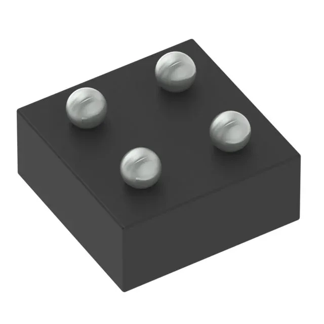
Single NAND gate in a 0.8 mm square package
The 32 mA output sink and source capability drives multiple CMOS loads or small LEDs directly, and the 4.3 ns propagation delay at 5V and 50 pF load keeps timing closure straightforward for most board-level glue logic.
Runs on any common logic rail
The 1.65V to 5.5V supply range means this gate works on 1.8V, 2.5V, 3.3V, or 5V rails without a separate level translator. Input logic thresholds scale with supply: low-level at 0.7V to 0.8V, high-level at 1.7V to 2V. That covers 3.3V CMOS and TTL-compatible levels cleanly. Quiescent current maxes at 10 µA, so it won't load down a battery-powered rail in standby.
Industrial temperature range — rated for the engine bay and the factory floor
No commercial-grade derating needed; the 74LVC family holds its timing and drive specs across the full range.
Tiny footprint — plan the solder paste and the stencil
The 4-XFDFN exposed-pad package (supplier device package 4-X2SON, 0.8x0.8 mm) is a leadless, no-lead package. Stencil aperture for the pad should match the recommended land pattern in the datasheet — too much paste and the part floats, too little and the thermal connection suffers.