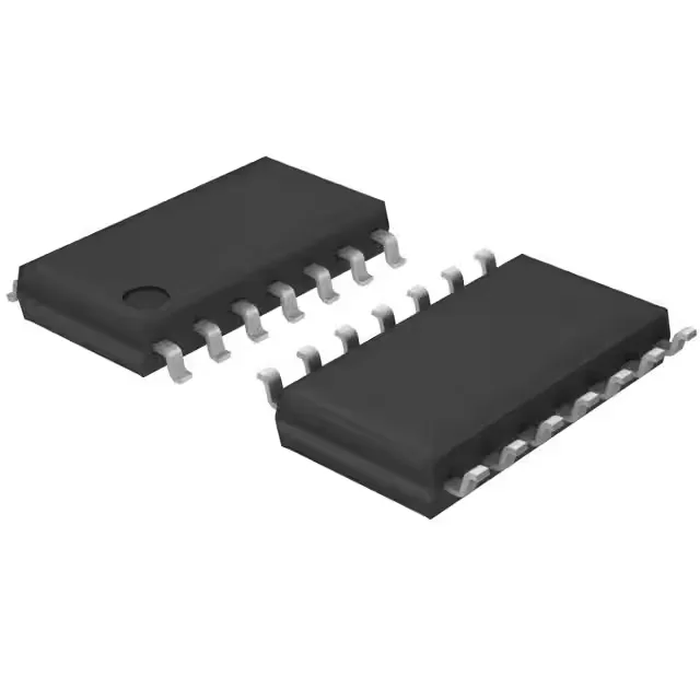
Texas Instruments SN74LVC10ANSR — Discrete Semiconductors

SN74LVC10ANSR Texas Instruments 74LVC Triple 3-Input NAND

MPNSN74LVC10ANSR
End of Life

Texas Instruments 74LVC series triple 3-input NAND gate, SN74LVC10ANSR, 14-SOIC package, 1.65V to 3.6V supply, -40°C to 125°C temperature range.

$0.56Ref. price · indicative, final on quote
Packaging14-SOIC (0.209", 5.30mm Width)
StockContact for availability
Lead timeIn Stock wk
MOQ1 pcs
  • 100% new & originalTraceable channels only — no refurbs, no pulls, no remarked parts.
  • Date & lot codes on quoteStated per line before you commit; label photos on request.
  • MSL-compliant ESD packingMoisture-sealed bags with indicator cards; reels photo-verified.
  • PayPal buyer protectionPay by T/T, PayPal or Payoneer — card payments covered end to end.

Specifications

SN74LVC10ANSR Technical Specifications
ParameterValue
Series74LVC
Logic typeNAND Gate
Mounting typeSurface Mount
Voltage1.65V ~ 3.6V
Current - quiescent1 µA
Current - output high, low24mA, 24mA
Number of inputs3
Operating temperature-40°C ~ 125°C
PackageTape & Reel (TR); Cut Tape (CT)
Case14-SOIC (0.209\", 5.30mm Width)
Number of circuits3
Input logic level - low0.7V ~ 0.8V
Input logic level - high1.7V ~ 2V
Max propagation delay @ v, max CL4.7ns @ 3.3V, 50pF

Product details

Triple 3-input NAND in the 74LVC family

The SN74LVC10ANSR: Three independent NAND gates, each with three inputs, are packaged in a 14-pin SOIC (0.209-inch body width, 5.30 mm) — the 14-SO footprint that mates with standard SOIC-14 land patterns. The supplier device package is designated 14-SO.

Supply voltage and temperature envelope

The input logic thresholds scale with VCC: low-level threshold is 0.7 V to 0.8 V, high-level threshold is 1.7 V to 2 V — so at 3.3 V VCC, a 1.8 V CMOS signal is still recognised as a logic high.

Speed and drive at 3.3 V

Maximum propagation delay is 4.7 ns at 3.3 V with a 50 pF load — this sets the data-rate ceiling for a single gate in a signal path. The 24 mA symmetric output drive (source and sink) can switch the 50 pF load with edge rates fast enough for 100+ MHz clock distribution in a point-to-point topology. Quiescent current is 1 µA max — the gates draw virtually no DC current when the inputs are static, which matters for battery-powered or power-sensitive designs where the logic sits idle most of the time.

Frequently asked questions

What compliance documentation does Texas Instruments provide for SN74LVC10ANSR?

The device is ROHS3 compliant. Standard Texas Instruments documentation includes the datasheet, RoHS certification, and REACH compliance reports available through the product page.