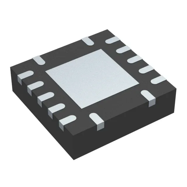
Quad 2-input AND gate in a 3.5×3.5 mm VQFN
Quiescent current is rated at 1 µA maximum, making this gate suitable for battery-backed or always-on sections where every microamp counts. Each output can sink or source 24 mA, enough to drive a standard CMOS load or a low-power LED indicator directly.
Maximum propagation delay is 3.9 ns at 3.3 V with a 50 pF load.
Active production, ROHS3, and the VQFN footprint
ROHS3 compliant. The 14-VQFN package measures 3.5 mm × 3.5 mm. The exposed pad requires a thermal-land pattern on the PCB.