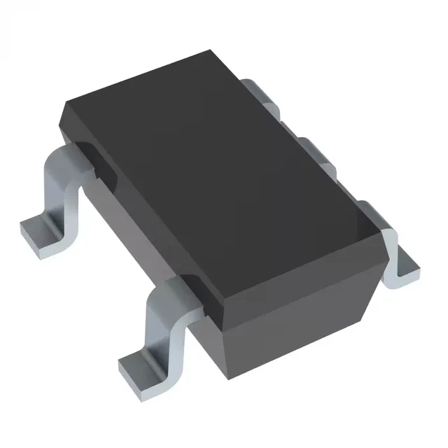
The SN74LV1T04DBVR: This wide VCC window lets it serve as a level translator in mixed-voltage systems — a 3.3 V-domain logic output can drive a 5 V input through the inverter's threshold, with the propagation delay settling in 7 ns at 5 V into a 30 pF load. The SOT-23-5 package (SC-74A) keeps the board footprint under 3 mm², fitting into dense mixed-signal layouts where a single inverter is needed for clock inversion, signal cleanup, or bus-hold logic.
Timing budget and output drive
Maximum propagation delay is 7 ns at 5 V with a 30 pF load — this sets the data-rate ceiling for the inverter path. At lower supply voltages the delay increases; the 1.6 V minimum supply still switches within the 74LV family's timing envelope, but the actual delay at 1.8 V is higher than the 5 V figure. The 8 mA source/sink capability at both rails means the output can drive up to five standard LSTTL loads or two 74HC inputs without slowing the edge rate. Quiescent current maxes at 10 µA across the full voltage and temperature range — relevant for battery-powered nodes where the inverter sits idle between switching events.
Active production — no lifecycle pressure
The 74LV series is a well-established low-voltage logic family with broad second-source coverage from multiple manufacturers. For BOM hedging, functionally equivalent single-gate inverters from the 74LVC or 74AHC series share the same SOT-23-5 footprint and supply range, though the logic thresholds and propagation delay differ — verify the timing closure against the specific downstream load.