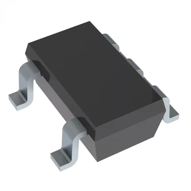
Texas Instruments SN74LV1T00DBVR — Analog & Data Acquisition

SN74LV1T00DBVR 74LV Single 2-Input NAND Gate, 1.6V-5.5V

MPNSN74LV1T00DBVR
End of Life

Texas Instruments 74LV series SN74LV1T00DBVR, single 2-input NAND gate, SC-74A SOT-753 surface mount, 1.6V to 5.5V supply, -40°C to 125°C, 8mA output, 7ns at 5V.

$0.53Ref. price · indicative, final on quote
PackagingSC-74A, SOT-753
StockContact for availability
MOQ1 pcs
  • 100% new & originalTraceable channels only — no refurbs, no pulls, no remarked parts.
  • Date & lot codes on quoteStated per line before you commit; label photos on request.
  • MSL-compliant ESD packingMoisture-sealed bags with indicator cards; reels photo-verified.
  • PayPal buyer protectionPay by T/T, PayPal or Payoneer — card payments covered end to end.

Specifications

SN74LV1T00DBVR Technical Specifications
ParameterValue
Series74LV
Logic typeNAND Gate
Mounting typeSurface Mount
Voltage1.6V ~ 5.5V
Current - quiescent10 µA
Current - output high, low8mA, 8mA
Number of inputs2
Operating temperature-40°C ~ 125°C (TA)
PackageTape & Reel (TR); Cut Tape (CT)
CaseSC-74A, SOT-753
Number of circuits1
Input logic level - low0.58V ~ 0.8V
Input logic level - high0.94V ~ 2.1V
Max propagation delay @ v, max CL7ns @ 5V, 30pF

Product details

Single NAND gate that bridges voltage domains

Its 1.6V to 5.5V supply range is the headline feature: this part acts as a voltage-level translator in addition to its logic function. A 1.8V input on the low side can drive a 3.3V or 5V output, and vice versa, without needing a separate level-shifter IC.

7 ns propagation delay — timing budget for mixed-voltage buses

At 5V with a 30pF load, the max propagation delay is 7 ns. The delay increases at lower supply voltages — the input logic thresholds shift with VCC, so a 1.8V system will see a longer propagation path. For timing closure, budget the worst-case delay at the actual operating voltage, not the 5V figure.

8 mA output drive — enough for a single load, not a bus

The output can sink or source 8 mA at both logic levels. That drives one standard CMOS input, a small LED through a series resistor, or the enable pin of a regulator. It will not drive a 50-ohm backplane or a bank of optocouplers without buffering. The 10 µA quiescent current is negligible for battery-powered designs.

It is ROHS3 compliant and remains a valid new-design choice. For production BOMs, the wide supply range and extended temperature grade make it a stable single-sourced line item; if dual-sourcing is required, the closest functional peer is the SN74AHC1G00DBVT, which has a narrower 2.0V to 5.5V supply range and a slightly different input threshold window.

Frequently asked questions

Can SN74LV1T00DBVR be used as a replacement for 74LVC1G00?

The SN74LV1T00DBVR is a functional replacement for the 74LVC1G00 in many designs, but check the input threshold voltages. The 74LV family has different VIH/VIL levels than the LVC family, so verify compatibility with the driving device's output levels at your operating voltage.