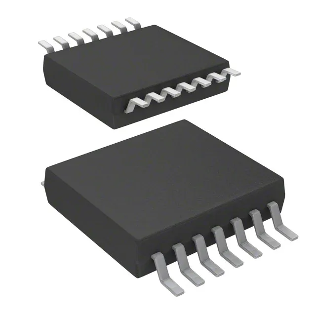
Texas Instruments SN74LV08ADGVR — Crystals & Oscillators

SN74LV08ADGVR Texas Instruments AND Gate IC 14-TVSOP

MPNSN74LV08ADGVR
End of Life

Texas Instruments 74LV series, AND Gate, 4 Circuit, 2 Input, 12mA output, 2V ~ 5.5V supply, -40°C ~ 125°C, 14-TVSOP package, SN74LV08ADGVR

$0.6Ref. price · indicative, final on quote
Packaging14-TFSOP (0.173", 4.40mm Width)
StockContact for availability
MOQ1 pcs
  • 100% new & originalTraceable channels only — no refurbs, no pulls, no remarked parts.
  • Date & lot codes on quoteStated per line before you commit; label photos on request.
  • MSL-compliant ESD packingMoisture-sealed bags with indicator cards; reels photo-verified.
  • PayPal buyer protectionPay by T/T, PayPal or Payoneer — card payments covered end to end.

Specifications

SN74LV08ADGVR Technical Specifications
ParameterValue
Series74LV
Logic typeAND Gate
Mounting typeSurface Mount
Voltage2V ~ 5.5V
Current - quiescent20 µA
Current - output high, low12mA, 12mA
Number of inputs2
Operating temperature-40°C ~ 125°C
PackageTape & Reel (TR); Cut Tape (CT)
Case14-TFSOP (0.173\", 4.40mm Width)
Number of circuits4
Input logic level - low0.5V
Input logic level - high1.5V
Max propagation delay @ v, max CL7.9ns @ 5V, 50pF

Product details

Quad 2-input AND gate in 14-TVSOP

The SN74LV08ADGVR is a Texas Instruments 74LV-series quad 2-input AND gate in a 14-TVSOP package. It operates from 2V to 5.5V, covering both 3.3V and 5V logic rails common in mixed-voltage BOMs.

Propagation delay and output drive

Maximum propagation delay is 7.9ns at 5V with a 50pF load, fast enough for most 10-20 MHz logic paths. Output sink and source current is 12mA each, sufficient for driving standard CMOS inputs and short PCB traces but not for LEDs or relays without a buffer.

Active production, no obsolescence concern

Sourced per RFQ against your BOM quantity.

Frequently asked questions

Can SN74LV08ADGVR be used at 3.3V?

Yes. The supply voltage range is 2V to 5.5V, so 3.3V is well within the operating window. Input logic levels are 0.5V low and 1.5V high at 3.3V supply, compatible with standard 3.3V CMOS and LVTTL families.

How does SN74LV08ADGVR differ from SN74LVC08AD?

The SN74LVC08AD is from the LVC family with 5V-tolerant inputs and a narrower temperature range (typically -40°C to 85°C). The LV family (SN74LV08ADGVR) operates up to 125°C and has a wider supply range, but its inputs are not 5V-tolerant above VCC. For a direct cross, the SN74LV08ADR (same die, different package) is the closest functional second-source.