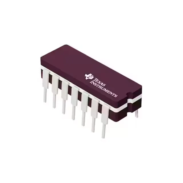
Texas Instruments SN74LS51N — Analog & Data Acquisition

SN74LS51N 74LS AND-OR-INVERT Gate, 14-DIP, 5V Supply

MPNSN74LS51N
End of Life

Texas Instruments SN74LS51N, 74LS series, dual 2-wide 2-input AND-OR-INVERT gate, 14-DIP (0.300", 7.62mm) through-hole package, 4.75V to 5.25V supply, 0°C to 70°C operating temperature.

$1.65Ref. price · indicative, final on quote
Packaging14-DIP (0.300", 7.62mm)
StockContact for availability
MOQ1 pcs
  • 100% new & originalTraceable channels only — no refurbs, no pulls, no remarked parts.
  • Date & lot codes on quoteStated per line before you commit; label photos on request.
  • MSL-compliant ESD packingMoisture-sealed bags with indicator cards; reels photo-verified.
  • PayPal buyer protectionPay by T/T, PayPal or Payoneer — card payments covered end to end.

Specifications

SN74LS51N Technical Specifications
ParameterValue
Series74LS
Logic typeAND/OR/INVERT Gate
Output typeSingle-Ended
Mounting typeThrough Hole
Voltage4.75V ~ 5.25V
Current - output high, low400µA, 8mA
Number of inputs10 Input (3, 3, 2, 2)
Operating temperature0°C ~ 70°C
PackageTube
Case14-DIP (0.300\", 7.62mm)
Number of circuits2
Schmitt trigger inputNo

Product details

What the SN74LS51N is and where it fits

The Texas Instruments SN74LS51N is a dual 2-wide 2-input AND-OR-INVERT gate from the 74LS low-power Schottky logic family. It integrates two independent circuits, each implementing the logic function (A AND B) OR (C AND D) then inverted, in a single 14-pin DIP package. This combinational gate is used for glue logic in 5V TTL systems — decoding, gating, or combining digital signals in legacy telecom, industrial controllers, test equipment, and prototyping boards where through-hole assembly is preferred.

Output drive and fan-out

The output is single-ended with a rated sink current of 8 mA and source current of 400 µA. The asymmetric drive is typical of 74LS: the output can sink a standard TTL load (one or two LS inputs) but sources very little. When driving a high-impedance CMOS input or an LED, use an external pull-up resistor or a buffer. The 400 µA source limit also means the high-level output voltage droops under even light loading — check the fan-out table in the datasheet if you are driving more than 10 LS loads.

Active production — sourcing reality

The SN74LS51N carries an Active lifecycle status. That said, 74LS is a mature logic family, and TI has consolidated production over the years — lead times and allocation can shift. We source this part through independent distribution, with each unit traceable back to the authorized chain.

Frequently asked questions

What are the output current ratings for SN74LS51N?

The output can sink 8 mA and source 400 µA. The high-level source current is limited, so driving more than a few LS inputs or any CMOS input without a pull-up may degrade the logic-high voltage.

What is the difference between SN74LS51N and 74LS51?

SN74LS51N is the full Texas Instruments order code for the 74LS51 dual AND-OR-INVERT gate in a 14-pin PDIP package. 74LS51 is a generic family designation; the exact part may come from different manufacturers with slight variations in package or temperature grade. The SN74LS51N is the TI-specified variant with commercial temperature range and through-hole DIP.