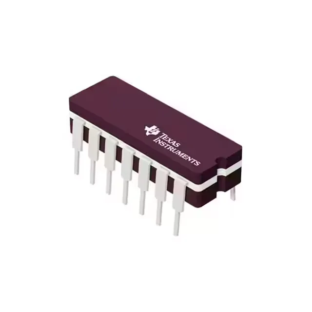
Texas Instruments SN74LS21N — Microcontrollers & Processors (MCU / MPU / DSP)

TI SN74LS21N Dual 4-Input AND Gate, 74LS, 20ns, 14-DIP

MPNSN74LS21N
End of Life

Texas Instruments 74LS series, AND Gate, SN74LS21N, 2 Circuits, 4 Inputs, 14-DIP (0.300", 7.62mm), Through Hole, Tube.

$0.91Ref. price · indicative, final on quote
Packaging14-DIP (0.300", 7.62mm)
RoHSROHS3 Compliant
Series74LS
Independent supplier — new & surplus stockAuthenticity-screened · ESD-safe packingListing updated Aug 2026

Specifications

SN74LS21N specifications
ParameterValue
Series74LS
Logic typeAND Gate
MountingThrough Hole
Supply voltage4.75V ~ 5.25V
Current - output high, low400µA, 8mA
I/O channels4
Operating temperature0°C ~ 70°C
PackageTube
Case14-DIP (0.300\", 7.62mm)
Number of circuits2
Input logic level - low0.8V
Input logic level - high2V
Max propagation delay @ v, max CL20ns @ 5V, 15pF

Product details

Dual 4-input AND gate in a 14-pin DIP

The SN74LS21N: It integrates two independent AND gates, each with four inputs, in a single 14-pin plastic DIP (0.300" body width) for through-hole assembly.

20 ns propagation delay at 5 V, 15 pF

Maximum propagation delay is 20 ns at 5 V supply and 15 pF load capacitance. This sets the timing floor for the signal path — at 5 V the gate toggles in under 20 ns, which is fast enough for most 5 V control logic but not for high-speed synchronous buses above 25 MHz. Output drive capability is 400 µA sourcing (logic high) and 8 mA sinking (logic low). The asymmetric drive means the gate can sink more current than it sources — common in TTL — so downstream loads should be designed to be driven low rather than high where possible. Input logic thresholds are 0.8 V maximum for a low and 2.0 V minimum for a high, compatible with standard 5 V TTL levels. The 0.8 V low threshold gives noise margin against ground bounce on a shared backplane.

Active production, ROHS3 compliant

ROHS3 compliant — no restricted substances above threshold limits. No additional compliance documentation (REACH, UL, IEC) is listed on the product record, so the standard TI declaration of conformity applies.

Frequently asked questions

What is the closest functional second-source to SN74LS21N?

It is not a pin-for-pin drop-in at 5 V because the HC family's input thresholds differ from TTL levels — at 5 V the HC low threshold is 1.5 V max vs 0.8 V for the LS part, so the HC gate may not recognise a TTL low signal correctly without a pull-up. The SN74ALS11ANS is a surface-mount 3-input AND gate in a different package and pinout, so it requires a board layout change.

What compliance documentation does Texas Instruments provide for SN74LS21N?

Texas Instruments provides ROHS3 compliance for the SN74LS21N. No UL, IEC, or REACH documentation is listed on the product record. Standard TI declarations of conformity and material composition data are available upon request through the supply chain.

Will SN74LS21N drop into a panel that was specified around SN74ALS11ANS without rewiring?

No. The SN74ALS11ANS is a surface-mount 14-pin SOIC package with a 3-input AND gate topology (three inputs per gate, three gates total), while the SN74LS21N is a through-hole 14-DIP with a 4-input AND gate (four inputs per gate, two gates total). The pinouts, package footprint, and logic function differ — a board spin is required.