Active production — what it means for a BOM line
The SN74LS20N: RoHS3 compliant, which covers the EU RoHS exemption list through 2024 — no separate exemption certificate is needed for most commercial and industrial assemblies.
The SN74LS20N is a dual 4-input NAND gate from the 74LS Schottky-clamped bipolar family. Maximum propagation delay is 15 ns at 5 V into a 15 pF load. This sets the data-path timing floor: for a 10 MHz clock, the gate adds one full period of delay, so the downstream setup time must budget for it. Output drive is 400 µA sourcing and 8 mA sinking — enough to drive one or two standard TTL loads, but not a high-fanout bus or a long unterminated trace without a buffer. Quiescent current is 800 µA maximum, typical for the 74LS family; the bipolar core draws steady supply current regardless of switching activity.
Package and board-fit — through-hole DIP
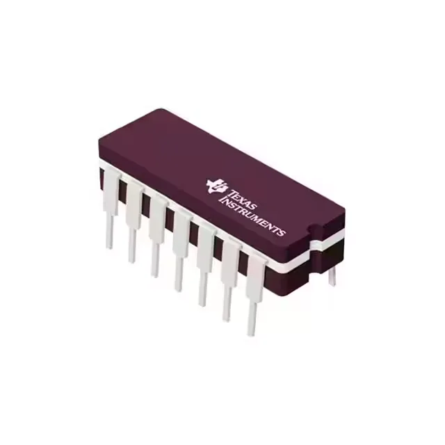
Housed in a 14-pin DIP with 0.300-inch (7.62 mm) row spacing, the SN74LS20N uses the standard 0.100-inch pitch through-hole footprint. The supplier device package is 14-PDIP.
Logic thresholds and noise margin
Input logic-low threshold is 0.8 V maximum; logic-high is 2 V minimum. With a 5 V supply, the low-level noise margin is about 0.8 V (from VIL max to the 0 V rail) and the high-level margin is about 3 V (from 2 V to 5 V). The four inputs per gate are internally pulled high through the 74LS input structure — unused inputs should be tied to VCC or a valid logic level, not left floating, to avoid oscillation and excess supply current.