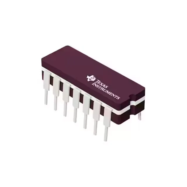
Quad 2-input AND gate with open-collector outputs
The SN74LS09N is a quad 2-input AND gate from the 74LS low-power Schottky family, with open-collector outputs that sink up to 8 mA per channel. This means the outputs can be wire-ANDed together or drive loads requiring a higher voltage than the logic supply — a common trick on legacy 5 V bus architectures where multiple gate outputs share a pull-up resistor. Propagation delay is 35 ns max at 5 V and 15 pF load, setting the practical data rate ceiling. For a 5 V logic system clocked at 10 MHz, the gate adds roughly one-third of a cycle of latency — fine for address decoding or control gating, but too slow for high-speed data paths where the 74F series would be a better fit.
Supply voltage and temperature envelope
If your board has drifted or uses a 5 V rail that sags below 4.75 V under load, the gate may not recognise a logic-high input (threshold is 2 V min). This part belongs in a conditioned indoor panel or lab bench, not an engine bay or freezer. The input-low threshold is 0.8 V max, input-high is 2 V min — standard TTL levels that interface cleanly with most 5 V CMOS and bipolar logic families.
Through-hole DIP for prototyping and repair
Housed in a 14-pin DIP with 0.300-inch (7.62 mm) body width, through-hole mount. This is the classic breadboard-friendly package — you can socket it, probe every pin, and swap it in seconds. For a repair bench tech, the scorch mark on a dead board often leads to a shorted output on one of these gates; swapping the DIP is a 30-second job with a desoldering station.